SLLSFP1A May   2024  – September 2024 TUSB521-Q1

PRODUCTION DATA  

  1.   1
  2. Features
  3. Applications
  4. Description
  5. Pin Configuration and Functions
  6. Specifications
    1. 5.1 Absolute Maximum Ratings
    2. 5.2 ESD Ratings
    3. 5.3 Recommended Operating Conditions
    4. 5.4 Thermal Information
    5. 5.5 Electrical Characteristics
    6. 5.6 Timing Requirements
    7. 5.7 Switching Characteristics
    8. 5.8 Typical Characteristics
  7. Parameter Measurement Information
  8. Detailed Description
    1. 7.1 Overview
    2. 7.2 Functional Block Diagram
    3. 7.3 Feature Description
      1. 7.3.1 USB 3.2
      2. 7.3.2 4-Level Inputs
      3. 7.3.3 Receiver Linear Equalization
    4. 7.4 Device Functional Modes
      1. 7.4.1 USB 3.2 2:1 MUX Description
      2. 7.4.2 Linear EQ Configuration
      3. 7.4.3 USB3.2 Modes
      4. 7.4.4 Operation Timing – Power Up
    5. 7.5 Programming
      1. 7.5.1 TUSB521-Q1 I2C Target Behavior
  9. Application and Implementation
    1. 8.1 Application Information
    2. 8.2 Typical Application
      1. 8.2.1 Design Requirements
      2. 8.2.2 Detailed Design Procedure
        1. 8.2.2.1 USB SSTX1/2 Receiver Configuration
        2. 8.2.2.2 USB RX1/2 Receiver Configuration
        3. 8.2.2.3 ESD Protection
      3. 8.2.3 Application Curve
    3. 8.3 Power Supply Recommendations
    4. 8.4 Layout
      1. 8.4.1 Layout Guidelines
      2. 8.4.2 Layout Example
  10. Register Maps
    1. 9.1 General Register (address = 0x0A) [reset = 00000001]
    2. 9.2 USB3.2 Control/Status Registers (address = 0x20) [reset = 00000000]
    3. 9.3 USB3.2 Control/Status Registers (address = 0x21) [reset = 00000000]
    4. 9.4 USB3.2 Control/Status Registers (address = 0x22) [reset = 00000000]
  11. 10Device and Documentation Support
    1. 10.1 Receiving Notification of Documentation Updates
    2. 10.2 Support Resources
    3. 10.3 Trademarks
    4. 10.4 Electrostatic Discharge Caution
    5. 10.5 Glossary
  12. 11Revision History
  13. 12Mechanical, Packaging, and Orderable Information

Typical Characteristics

TUSB521-Q1 USB RX1 EQ Settings Curves
Figure 5-1 USB RX1 EQ Settings Curves
TUSB521-Q1 USB SSTX EQ Settings Curves
Figure 5-3 USB SSTX EQ Settings Curves
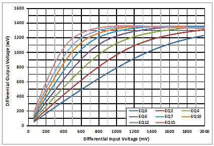
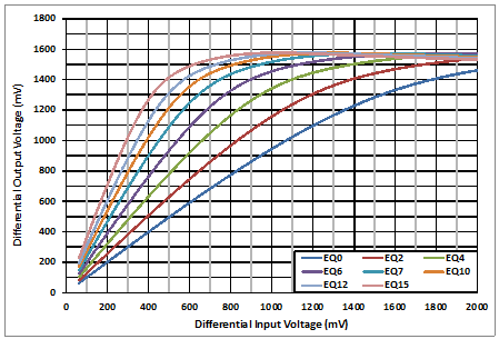
TUSB521-Q1 USB SSTX Linearity Curves at 2.5GHz
Figure 5-5 USB SSTX Linearity Curves at 2.5GHz
TUSB521-Q1 Input Return Loss Performance
Figure 5-7 Input Return Loss Performance
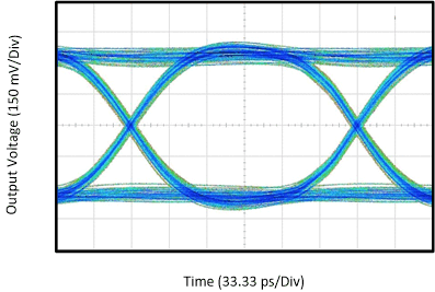
TUSB521-Q1 USB 3.2 Gen1 Eye-Pattern Performance with 12-inch Input PCB Trace at 5Gbps
Figure 5-9 USB 3.2 Gen1 Eye-Pattern Performance with 12-inch Input PCB Trace at 5Gbps
TUSB521-Q1 USB3 RX1 EQ0 and EQ15 Across Temperature
Figure 5-2 USB3 RX1 EQ0 and EQ15 Across Temperature
TUSB521-Q1 USB3 SSTX SSEQ0 and SSEQ15 Across Temperature
Figure 5-4 USB3 SSTX SSEQ0 and SSEQ15 Across Temperature
TUSB521-Q1 USB RX1 Linearity Curves at 2.5GHz
Figure 5-6 USB RX1 Linearity Curves at 2.5GHz
TUSB521-Q1 Output Return Loss Performance
Figure 5-8 Output Return Loss Performance