SLLSFQ9B May   2024  – October 2024 THVD2410V-EP , THVD2450V-EP , THVD2452V-EP

PRODUCTION DATA  

  1.   1
  2. Features
  3. Applications
  4. Description
  5. Pin Configuration and Functions
  6. Specifications
    1. 5.1  Absolute Maximum Ratings
    2. 5.2  ESD Ratings
    3. 5.3  ESD Ratings [IEC]
    4. 5.4  Recommended Operating Conditions
    5. 5.5  Thermal Information
    6. 5.6  Power Dissipation
    7. 5.7  Electrical Characteristics
    8. 5.8  Switching Characteristics - 250 kbps
    9. 5.9  Switching Characteristics - 1 Mbps
    10. 5.10 Switching Characteristics - 20 Mbps
    11. 5.11 Switching Characteristics - 50 Mbps
    12. 5.12 Typical Characteristics
  7. Parameter Measurement Information
  8. Detailed Description
    1. 7.1 Overview
    2. 7.2 Functional Block Diagrams
    3. 7.3 Feature Description
      1. 7.3.1 ±70-V Fault Protection
      2. 7.3.2 Integrated IEC ESD and EFT Protection
      3. 7.3.3 Driver Overvoltage and Overcurrent Protection
      4. 7.3.4 Enhanced Receiver Noise Immunity
      5. 7.3.5 Receiver Fail-Safe Operation
      6. 7.3.6 Low-Power Shutdown Mode
    4. 7.4 Device Functional Modes
  9. Application and Implementation
    1. 8.1 Application Information
    2. 8.2 Typical Application
      1. 8.2.1 Design Requirements
        1. 8.2.1.1 Data Rate and Bus Length
        2. 8.2.1.2 Stub Length
        3. 8.2.1.3 Bus Loading
        4. 8.2.1.4 Transient Protection
      2. 8.2.2 Detailed Design Procedure
      3. 8.2.3 Application Curves
    3. 8.3 Power Supply Recommendations
    4. 8.4 Layout
      1. 8.4.1 Layout Guidelines
      2. 8.4.2 Layout Example
  10. Device and Documentation Support
    1. 9.1 Device Support
      1. 9.1.1 Third-Party Products Disclaimer
    2. 9.2 Receiving Notification of Documentation Updates
    3. 9.3 Support Resources
    4. 9.4 Trademarks
    5. 9.5 Electrostatic Discharge Caution
    6. 9.6 Glossary
  11. 10Revision History
  12. 11Mechanical, Packaging, and Orderable Information

Typical Characteristics

THVD2410V-EP THVD2450V-EP THVD2452V-EP Driver Output Voltage vs Driver Output Current
DE = VCC D = 0V TA = 25 °C
Figure 5-1 Driver Output Voltage vs Driver Output Current
THVD2410V-EP THVD2450V-EP THVD2452V-EP Driver Output Current vs Supply Voltage
TA = 25 °C DE = D = VCC RL = 54Ω
Figure 5-3 Driver Output Current vs Supply Voltage
THVD2410V-EP THVD2450V-EP THVD2452V-EP THVD2410V-EP Driver Propagation Delay vs Temperature

Figure 5-5 THVD2410V-EP Driver Propagation Delay vs Temperature
THVD2410V-EP THVD2450V-EP THVD2452V-EP THVD2450V-EP: 50Mbps Driver Rise or Fall Time vs Temperature
Figure 5-7 THVD2450V-EP: 50Mbps Driver Rise or Fall Time vs Temperature
THVD2410V-EP THVD2450V-EP THVD2452V-EP Driver Differential Output voltage vs Driver Output Current
DE = VCC D = 0V TA = 25 °C
Figure 5-2 Driver Differential Output voltage vs Driver Output Current
THVD2410V-EP THVD2450V-EP THVD2452V-EP THVD2410V-EP Driver Rise or Fall Time vs Temperature
Figure 5-4 THVD2410V-EP Driver Rise or Fall Time vs Temperature
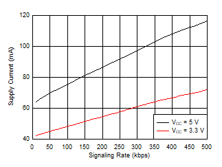
THVD2410V-EP THVD2450V-EP THVD2452V-EP THVD2410V-EP Supply Current vs Signal Rate
TA = 25 °C RL = 54Ω
Figure 5-6 THVD2410V-EP Supply Current vs Signal Rate
THVD2410V-EP THVD2450V-EP THVD2452V-EP THVD2450V-EP: 50Mbps Driver Propagation Delay vs Temperature
Figure 5-8 THVD2450V-EP: 50Mbps Driver Propagation Delay vs Temperature