SLLSFS3 May 2024 MCT8316A-Q1
PRODUCTION DATA
- 1
- 1 Features
- 2 Applications
- 3 Description
- 4 Pin Configuration and Functions
- 5 Specifications
-
6 Detailed Description
- 6.1 Overview
- 6.2 Functional Block Diagram
- 6.3
Feature Description
- 6.3.1 Output Stage
- 6.3.2 Device Interface Modes
- 6.3.3 Step-Down Mixed-Mode Buck Regulator
- 6.3.4 AVDD Linear Voltage Regulator
- 6.3.5 Charge Pump
- 6.3.6 Slew Rate Control
- 6.3.7 Cross Conduction (Dead Time)
- 6.3.8 SPEED Control
- 6.3.9 Starting the Motor Under Different Initial Conditions
- 6.3.10 Motor Start Sequence (MSS)
- 6.3.11 Closed Loop Operation
- 6.3.12 Speed Loop
- 6.3.13 Input Power Regulation
- 6.3.14 Anti-Voltage Surge (AVS)
- 6.3.15 Output PWM Switching Frequency
- 6.3.16 Fast Start-up (< 50 ms)
- 6.3.17 Fast Deceleration
- 6.3.18 Active Demagnetization
- 6.3.19 Motor Stop Options
- 6.3.20 FG Configuration
- 6.3.21
Protections
- 6.3.21.1 VM Supply Undervoltage Lockout
- 6.3.21.2 AVDD Undervoltage Lockout (AVDD_UV)
- 6.3.21.3 BUCK Undervoltage Lockout (BUCK_UV)
- 6.3.21.4 VCP Charge Pump Undervoltage Lockout (CPUV)
- 6.3.21.5 Overvoltage Protection (OVP)
- 6.3.21.6 Overcurrent Protection (OCP)
- 6.3.21.7 Buck Overcurrent Protection
- 6.3.21.8
Cycle-by-Cycle (CBC) Current Limit (CBC_ILIMIT)
- 6.3.21.8.1 CBC_ILIMIT Automatic Recovery next PWM Cycle (CBC_ILIMIT_MODE = 000xb)
- 6.3.21.8.2 CBC_ILIMIT Automatic Recovery Threshold Based (CBC_ILIMIT_MODE = 001xb)
- 6.3.21.8.3 CBC_ILIMIT Automatic Recovery after 'n' PWM Cycles (CBC_ILIMIT_MODE = 010xb)
- 6.3.21.8.4 CBC_ILIMIT Report Only (CBC_ILIMIT_MODE = 0110b)
- 6.3.21.8.5 CBC_ILIMIT Disabled (CBC_ILIMIT_MODE = 0111b or 1xxxb)
- 6.3.21.9 Lock Detection Current Limit (LOCK_ILIMIT)
- 6.3.21.10 Thermal Warning (OTW)
- 6.3.21.11 Thermal Shutdown (TSD)
- 6.3.21.12 Motor Lock (MTR_LCK)
- 6.3.21.13 Motor Lock Detection
- 6.3.21.14 IPD Faults
- 6.4 Device Functional Modes
- 6.5 External Interface
- 6.6 EEPROM access and I2C interface
- 6.7 EEPROM (Non-Volatile) Register Map
- 6.8 RAM (Volatile) Register Map
- 7 Application and Implementation
- 8 Device and Documentation Support
- 9 Revision History
- 10Mechanical, Packaging, and Orderable Information
6.3.6 Slew Rate Control
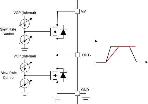
An adjustable gate-drive current control for the MOSFETs in the output stage is provided to achieve configurable slew rate for EMI mitigation. The MOSFET VDS slew rate is a critical factor for optimizing radiated emissions, total energy and duration of diode recovery spikes and switching voltage transients related to parasitic elements of the PCB. This slew rate is predominantly determined by the control of the internal MOSFET gate current as shown in Figure 6-9.
 Figure 6-9 Slew Rate Circuit Implementation
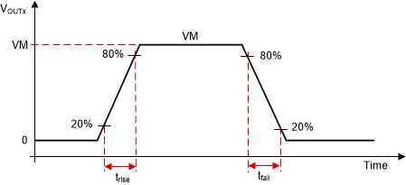
The slew rate of each half-bridge can be adjusted through SLEW_RATE settings. Slew rate can be configured as 25-V/µs, 50-V/µs, 125-V/µs or 200-V/µs. The slew rate is calculated by the rise-time and fall-time of the voltage on OUTx pin as shown in Figure 6-10.
 Figure 6-10 Slew Rate
Timings