SLLU149E June   2011  – February 2016 TUSB7320 , TUSB7340


  1.   TUSB73x0 Board Design and Layout Guidelines
    1.     Trademarks
    2.     Related Documentation
  2. Typical System Implementation
    1. 1.1 Overview
  3. Power
    1. 2.1 Overview
    2. 2.2 Digital Supplies
    3. 2.3 Analog Supplies
    4. 2.4 Ground Terminal
    5. 2.5 Capacitor Selection Recommendations
    6. 2.6 USB VBUS
  4. Device Reset
    1. 3.1 Overview
  5. General High Speed Layout Guidelines
    1. 4.1 Printed Circuit Board Stackup (FR-4 Example)
    2. 4.2 Return Current and Plane References
    3. 4.3 Split Planes – What to Avoid
    4. 4.4 Avoiding Crosstalk
  6. USB Connection
    1. 5.1 Overview
    2. 5.2 Internal Chip Trace Length Mismatch
    3. 5.3 High-Speed Differential Routing
    4. 5.4 SuperSpeed Differential Routing
  7. Package and Breakout
    1. 6.1 Package Drawing
    2. 6.2 Routing Between Pads
    3. 6.3 Pads
    4. 6.4 Land Pattern Recommendation
    5. 6.5 Solder Stencil
  8. PCI Express Connection
    1. 7.1 Internal Chip Trace Length Mismatch
    2. 7.2 Transmit and Receive Links
    3. 7.3 PCI-Express Reference Clock Input
    4. 7.4 PCI Express Reset
    5. 7.5 PCI Express WAKE/CLKREQ
      1. 7.5.1 Leakage Current on Pins WAKE# and CLKREQ#
      2. 7.5.2 Recommendations
  9. Wake from S3
    1. 8.1 Overview
  10. Device Input Clock
    1. 9.1 Overview
  11. 10JTAG Interface
    1. 10.1 Overview
  12. 11Differential Pair ESD Protection
    1. 11.1 Overview
  13. 12SuperSpeed Redriver
    1. 12.1 Overview
  14. 13SMI Pin Implementation
    1. 13.1 Overview
  15. 14Schematics
    1. 14.1 Overview
    2. 14.2 TUSB7320 DEMO EVM REVB Schematics
    3. 14.3 TUSB7340 DEMO EVM REVB Schematics
  16.   Revision History

Overview

See Achieving_Lowest_Power_with_TUSB73X0.pdf for more information on the settings used to get these low power numbers.
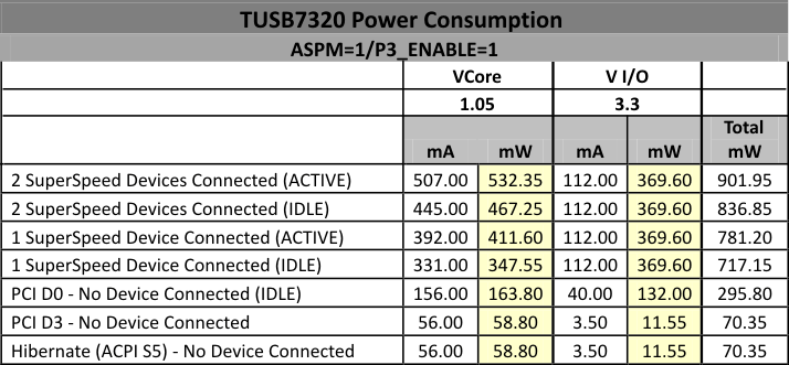
pwr_consumption_20_llu149.gifFigure 2-1 TUSB7320 Power Consumption
pwr_consumption_40_llu149.epsFigure 2-2 TUSB7340 Power Consumption