Understanding Operational Amplifier Specifications
1 Introduction
The term operational amplifier, abbreviated op amp, was coined in the 1940s to refer to a special kind of amplifier that, by proper selection of external components, can be configured to perform a variety of mathematical operations. Early op amps were made from vacuum tubes consuming lots of space and energy. Later op amps were made smaller by implementing them with discrete transistors. Today, op amps are monolithic integrated circuits, highly efficient and cost effective.
1.1 Amplifier Basics
Before jumping into op amps, lets take a minute to review some amplifier fundamentals. An amplifier has an input port and an output port. In a linear amplifier, output signal = A × input signal, where A is the amplification factor or gain.
Depending on the nature of input and output signals, we can have four types of amplifier gain:
- Voltage (voltage out/voltage in)
- Current (current out/current in)
- Transresistance (voltage out/current in)
- Transconductance (current out/voltage in)
Since most op amps are voltage amplifiers, we will limit our discussion to voltage amplifiers.
Thevenin’s theorem can be used to derive a model of an amplifier, reducing it to the appropriate voltage sources and series resistances. The input port plays a passive role, producing no voltage of its own, and its Thevenin equivalent is a resistive element, Ri. The output port can be modeled by a dependent voltage source, AVi, with output resistance, Ro. To complete a simple amplifier circuit, we will include an input source and impedance, Vs and Rs, and output load, RL. Figure 1-1 shows the Thevenin equivalent of a simple amplifier circuit.
 Figure 1-1 Thevenin Model of Amplifier with Source Load
It can be seen that we have voltage divider circuits at both the input port and the output port of the amplifier. This requires us to re-calculate whenever a different source and/or load is used and complicates circuit calculations.
1.2 Ideal Op Amp Model
The Thevenin amplifier model shown in Figure 1-1 is redrawn in Figure 1-2 showing standard op amp notation. An op amp is a differential to single-ended amplifier. It amplifies the voltage difference, Vd = Vp - Vn, on the input port and produces a voltage, Vo, on the output port that is referenced to ground.
 Figure 1-2 Standard Op Amp Notation
We still have the loading effects at the input and output ports as noted above. The ideal op amp model was derived to simplify circuit calculations and is commonly used by engineers in first-order approximation calculations. The ideal model makes three simplifying assumptions:
- Gain is infinite
Equation 1. a = ∞
- Input resistance is infinite
Equation 2. Ri = ∞
- Output resistance is zero
Equation 3. Ro = 0
Applying these assumptions to Figure 1-2 results in the ideal op amp model shown in Figure 1-3.
 Figure 1-3 Ideal Op Amp Model
Other simplifications can be derived using the ideal op amp model:
Because Ri = ∞, we assume In = Ip = 0. There is no loading effect at the input.
Because Ro = 0 there is no loading effect at the output.
If the op amp is in linear operation, V0 must be a finite voltage. By definition Vo = Vd × a. Rearranging, Vd = Vo / a . Since a = ∞, Vd = Vo / ∞ = 0. This is the basis of the virtual short concept.
The ideal voltage source driving the output port depends only on the voltage difference across its input port. It rejects any voltage common to Vn and Vp.
No frequency dependencies are assumed.
There are no changes in performance over time, temperature, humidity, power supply variations, etc.
2 Non-Inverting Amplifier
An ideal op amp by itself is not a very useful device since any finite input signal would result in infinite output. By connecting external components around the ideal op amp, we can construct useful amplifier circuits. Figure 2-1 shows a basic op amp circuit, the non-inverting amplifier. The triangular gain block symbol is used to represent an ideal op amp. The input terminal marked with a + (Vp) is called the non-inverting input; – (Vn) marks the inverting input.
 Figure 2-1 Non-Inverting
Amplifier
Figure 2-1 Non-Inverting
AmplifierTo understand this circuit we must derive a relationship between the input voltage, Vi, and the output voltage, Vo.
Remembering that there is no loading at the input,
The voltage at Vn is derived from Vo via the resistor network, R1 and R2, so that,
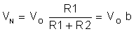
where,
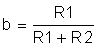
The parameter b is called the feedback factor because it represents the portion of the output that is fed back to the input.
Recalling the ideal model,
Substituting,
and collecting terms yield,
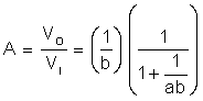
This result shows that the op amp circuit of Figure 2-1 is itself an amplifier with gain A. Since the polarity of Vi and VO are the same, it is referred to as a non-inverting amplifier.
A is called the close loop gain of the op amp circuit, whereas a is the open loop gain. The product ab is called the loop gain. This is the gain a signal would see starting at the inverting input and traveling in a clockwise loop through the op amp and the feedback network.