SLOA011B January 2018 – July 2021 LF347 , LF353 , LM348 , MC1458 , TL022 , TL061 , TL062 , TL071 , TL072 , UA741
- 1Introduction
- 2Non-Inverting Amplifier
- 3Inverting Amplifier
- 4Simplified Op Amp Circuit Diagram
-
5Op Amp Specifications
- 5.1 Absolute Maximum Ratings and Recommended Operating Condition
- 5.2 Input Offset Voltage
- 5.3 Input Current
- 5.4 Input Common Mode Voltage Range
- 5.5 Differential Input Voltage Range
- 5.6 Maximum Output Voltage Swing
- 5.7 Large Signal Differential Voltage Amplification
- 5.8 Input Parasitic Elements
- 5.9 Output Impedance
- 5.10 Common-Mode Rejection Ratio
- 5.11 Supply Voltage Rejection Ratio
- 5.12 Supply Current
- 5.13 Slew Rate at Unity Gain
- 5.14 Equivalent Input Noise
- 5.15 Total Harmonic Distortion Plus Noise
- 5.16 Unity-Gain Bandwidth and Phase Margin
- 5.17 Settling Time
- 6References
- 7Glossary
- 8Revision History
5.4 Input Common Mode Voltage Range
Normally there is a voltage that is common to the inputs of the op amp. If this common mode voltage gets too high or too low, the inputs will shut down and proper operation ceases. The common mode input voltage range, VICR, specifies the range over which normal operation is guaranteed.
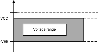
Figure 5-2 illustrates the positive input voltage limit using the simplified op amp diagram of Figure 4-1. When VIN is higher than VCC - 0.9 V, the input transistors and the current source will begin to shut down.
 Figure 5-2 Positive Common-Mode Voltage Input Limit
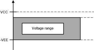
Figure 5-3 illustrates the negative input voltage limit using the simplified op amp diagram of Figure 4-1. When VIN is less than –VEE + 0.6 V, the current mirror (Q3 - Q4) will begin to shut down.
 Figure 5-3 Negative Common-Mode Input Limit
Structures like the one shown in the example above do not allow the common-mode input voltage to include either power supply rail. Other technologies used to construct op amp inputs offer different common-mode input voltage ranges that do include one or both power supply rails. Some examples are as follows (reference schematics can be found in the Texas Instruments’ data book, Amplifiers, Comparators, and Special Functions):
- The LM324 and LM358 use bipolar PNP inputs that have their collectors connected to the negative power rail. Since VBC can equal zero, this allows the common-mode input voltage range to include the negative power rail.
- The TL07X and TLE207X type BiFET op amps use p-channel JFET inputs with the sources tied to the positive power rail via a bipolar current source. Since VGS can equal zero, this structure typically allows the common-mode input voltage range to include the positive power rail.

- TI LinCMOS op amps use pchannel CMOS inputs with the substrate tied to the positive power rail. Therefore, a conducting channel is created for VG + VTH < VDD and this allows the common-mode input voltage to include the negative power rail.
- Rail-to-rail input op amps use complementary N and P type devices in the differential inputs. When the common-mode input voltage nears either rail at least one of the differential inputs is still active.
