SLOA059B October 2022 – March 2023 OPA2991 , TLC2654 , TLC4502 , TLE2021 , TLV2721
2 Input Offset Voltage Defined
The input offset voltage (VOS) is defined as the voltage that must be applied between the two input terminals of the op amp to obtain zero volts at the output. VOS is symbolically represented by a voltage source that is in series with either the positive or negative input terminal (it is mathematically equivalent either way). VOS is considered to be a DC error and is present from the moment that power is applied until it is turned off, with or without an input signal. It occurs during the biasing of the op amp and its effect can only be reduced, not eliminated.
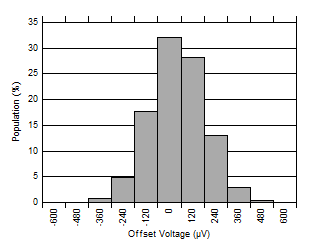
It can be either negative or positive in polarity and can vary from device to device (die to die) of the same wafer lot. Figure 2-1 shows the distribution of VOS measured in one wafer lot of the OPA2991 op amp as an example of the variance that VOS can have.
 Figure 2-1 Distribution of VOS for the OPA2991