SLOS073H March   1976  – October 2024 RC4558

PRODUCTION DATA  

  1.   1
  2. Features
  3. Applications
  4. Description
  5. Pin Configuration and Functions
  6. Specifications
    1. 5.1 Absolute Maximum Ratings
    2. 5.2 ESD Ratings
    3. 5.3 Recommended Operating Conditions
    4. 5.4 Thermal Information
    5. 5.5 Electrical Characteristics
    6. 5.6 Typical Characteristics
  7. Detailed Description
    1. 6.1 Overview
    2. 6.2 Functional Block Diagram
    3. 6.3 Feature Description
      1. 6.3.1 Unity-Gain Bandwidth
      2. 6.3.2 Common-Mode Rejection Ratio
      3. 6.3.3 Slew Rate
    4. 6.4 Device Functional Modes
  8. Application and Implementation
    1. 7.1 Application Information
    2. 7.2 Typical Application
      1. 7.2.1 Design Requirements
      2. 7.2.2 Detailed Design Procedure
        1. 7.2.2.1 Amplifier Selection
        2. 7.2.2.2 Passive Component Selection
      3. 7.2.3 Application Curves
    3. 7.3 Power Supply Recommendations
    4. 7.4 Layout
      1. 7.4.1 Layout Guidelines
      2. 7.4.2 Layout Example
  9. Device and Documentation Support
    1. 8.1 Trademarks
    2. 8.2 Electrostatic Discharge Caution
    3. 8.3 Glossary
  10. Revision History
  11. 10Mechanical, Packaging, and Orderable Information

Typical Application

Some applications require differential signals. Figure 7-1 shows a simple circuit to convert a single-ended input of 2V to 10V into differential output of ±8V on a single 15V supply. The output range is intentionally limited to maximize linearity. The circuit is composed of two amplifiers. One amplifier acts as a buffer and creates a voltage, VOUT+. The second amplifier inverts the input and adds a reference voltage to generate VOUT–. Both VOUT+ and VOUT– range from 2V to 10V. The difference, VDIFF, is the difference between VOUT+ and VOUT–.
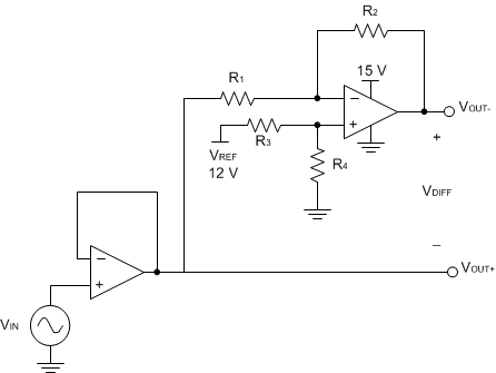
RC4558 Schematic for Single-Ended Input to Differential Output ConversionFigure 7-1 Schematic for Single-Ended Input to Differential Output Conversion