SLOS073H March   1976  – October 2024 RC4558

PRODUCTION DATA  

  1.   1
  2. Features
  3. Applications
  4. Description
  5. Pin Configuration and Functions
  6. Specifications
    1. 5.1 Absolute Maximum Ratings
    2. 5.2 ESD Ratings
    3. 5.3 Recommended Operating Conditions
    4. 5.4 Thermal Information
    5. 5.5 Electrical Characteristics
    6. 5.6 Typical Characteristics
  7. Detailed Description
    1. 6.1 Overview
    2. 6.2 Functional Block Diagram
    3. 6.3 Feature Description
      1. 6.3.1 Unity-Gain Bandwidth
      2. 6.3.2 Common-Mode Rejection Ratio
      3. 6.3.3 Slew Rate
    4. 6.4 Device Functional Modes
  8. Application and Implementation
    1. 7.1 Application Information
    2. 7.2 Typical Application
      1. 7.2.1 Design Requirements
      2. 7.2.2 Detailed Design Procedure
        1. 7.2.2.1 Amplifier Selection
        2. 7.2.2.2 Passive Component Selection
      3. 7.2.3 Application Curves
    3. 7.3 Power Supply Recommendations
    4. 7.4 Layout
      1. 7.4.1 Layout Guidelines
      2. 7.4.2 Layout Example
  9. Device and Documentation Support
    1. 8.1 Trademarks
    2. 8.2 Electrostatic Discharge Caution
    3. 8.3 Glossary
  10. Revision History
  11. 10Mechanical, Packaging, and Orderable Information

Application Curves

The measured transfer functions in Figure 7-2, Figure 7-3, and Figure 7-4 were generated by sweeping the input voltage from 0V to 12V. However, this design must only be used between 2V and 10V for optimum linearity.
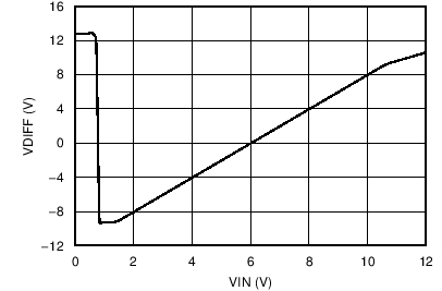
RC4558 Differential Output Voltage Node vs Input VoltageFigure 7-2 Differential Output Voltage Node vs Input Voltage
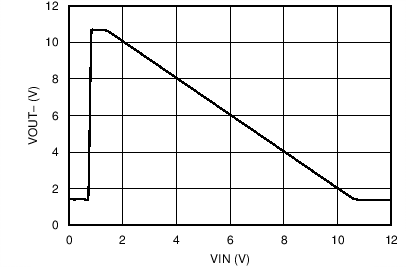
RC4558 Positive Output Voltage Node vs Input VoltageFigure 7-4 Positive Output Voltage Node vs Input Voltage
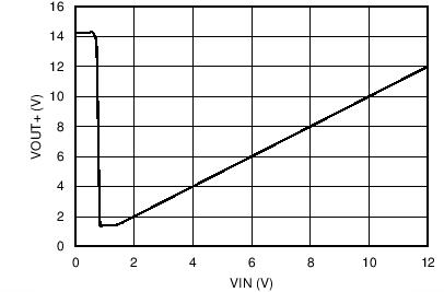
RC4558 Positive Output Voltage Node vs Input VoltageFigure 7-3 Positive Output Voltage Node vs Input Voltage