SLOS265F August 1999 – July 2024 THS4021 , THS4022
PRODUCTION DATA
- 1
- 1 Features
- 2 Applications
- 3 Description
- 4 Pin Configuration and Functions
-
5 Specifications
- 5.1 Absolute Maximum Ratings
- 5.2 ESD Ratings
- 5.3 Recommended Operating Conditions
- 5.4 Thermal Information - THS4021
- 5.5 Thermal Information - THS4022
- 5.6 Electrical Characteristics - THS4021D and THS4022DGN
- 5.7 Electrical Characteristics - THS4021DGN
- 5.8 Typical Characteristics: THS4021D and THS4022DGN
- 5.9 Typical Characteristics: THS4021DGN
- 6 Detailed Description
- 7 Application and Implementation
- 8 Device and Documentation Support
- 9 Revision History
- 10Mechanical, Packaging, and Orderable Information
5.9 Typical Characteristics: THS4021DGN
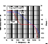 Figure 5-32 Open Loop Gain and Phase
Response vs Frequency
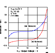 Figure 5-34 Distortion vs Output
Voltage
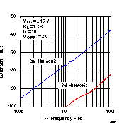 Figure 5-36 Distortion vs
Frequency
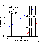 Figure 5-38 Distortion vs
Frequency
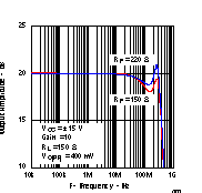 Figure 5-40 Output Amplitude vs
Frequency
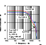 Figure 5-42 Output Amplitude vs
Frequency
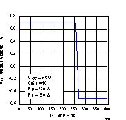 Figure 5-44 1-V Step Response
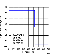 Figure 5-46 1-V Step Response
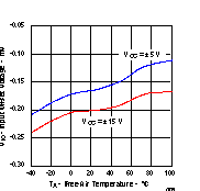 Figure 5-48 Input Offset Voltage vs
Free-air Temperature
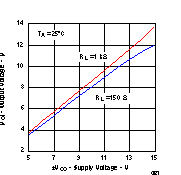 Figure 5-50 Output Voltage vs Supply
Voltage
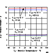 Figure 5-52 Output Voltage vs Free-air
Temperature
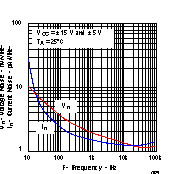 Figure 5-54 Voltage and Current Noise
vs Frequency
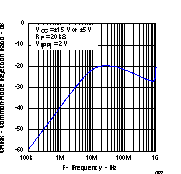 Figure 5-56 Common Mode Rejection
Ratio vs Frequency
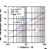 Figure 5-33 Total Harmonic Distortion
vs Frequency
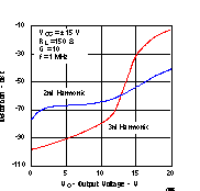 Figure 5-35 Distortion vs Output
Voltage
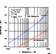 Figure 5-37 Distortion vs
Frequency
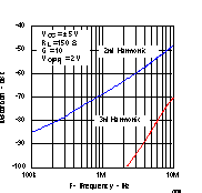 Figure 5-39 Distortion vs
Frequency
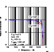 Figure 5-41 Output Amplitude vs
Frequency
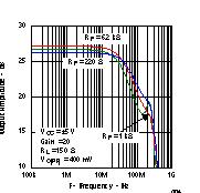 Figure 5-43 Output Amplitude vs
Frequency
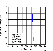 Figure 5-45 5-V Step Response
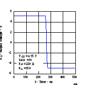 Figure 5-47 10-V Step Response
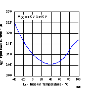 Figure 5-49 Input Bias Current vs
Free-air Temperature
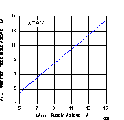 Figure 5-51 Common-mode Input Voltage
vs Supply Voltage
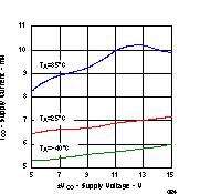 Figure 5-53 Supply Current vs Supply
Voltage
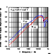 Figure 5-55 Power Supply Rejection
Ratio vs Frequency