DATA SHEET
TLV320AIC3256 Ultra Low Power Stereo Audio Codec With Embedded miniDSP
1 Features
- Stereo Audio DAC with 100dB SNR
- 5.0mW Stereo 48ksps DAC-to-Ground-Centered Headphone Playback
- Stereo Audio ADC with 93dB SNR
- 5.2mW Stereo 48ksps ADC Record
- PowerTune™
- Extensive Signal Processing Options
- Embedded miniDSP
- Six Single-Ended or 3 Fully-Differential Analog Inputs
- Stereo Analog and Digital Microphone Inputs
- Ground-Centered Stereo Headphone Outputs
- Very Low-Noise PGA
- Low Power Analog Bypass Mode
- Programmable Microphone Bias
- Programmable PLL
- 5mm x 5mm 40-pin QFN Package or 3.5mm x 3.3mm 42-ball WCSP
2 Applications
- Portable Navigation Devices (PND)
- Portable Media Player (PMP)
- Mobile Handsets
- Communication
- Portable Computing
- Advanced DSP algorithms
3 Description
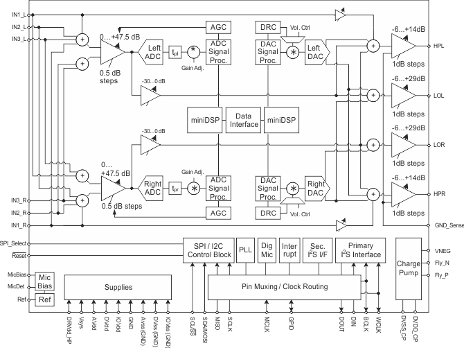
The TLV320AIC3256 (also called the AIC3256) is a flexible, low-power, low-voltage stereo audio codec with programmable inputs and outputs, PowerTune capabilities, fully-programmable miniDSP, fixed predefined and parameterizable signal processing blocks, integrated PLL, and flexible digital interfaces.
Device Information(1)
| PART NUMBER | PACKAGE | BODY SIZE (NOM) |
|---|---|---|
| TLV320AIC3256 | WQFN (40) | 5.00 mm x 5.00 mm |
| DSBGA (42) | 3.49 mm x 3.29 mm |
- For all available packages, see the orderable addendum at the end of the datasheet.
4 Simplified Block Diagram
5 Revision History
Changes from B Revision (January 2013) to C Revision
- Added the Device information table, Handling Ratings table, Applications and Implementation section, Layout section, and the Device and Documentation Support sectionGo
- Deleted "Acoustic Echo Cancellation (AEC)" and "Active Noise Cancellation (ANC)" from applications listGo
- Added Note 1 to the Pin Functions tableGo
- Added "Audio input mux ac signal swing" to the Recommended Operating Conditions table Go
- Added the Digital Microphone PDM Timing (see ) sectionGo
Changes from A Revision (December 2010) to B Revision
- Added WCSP package (YZF)Go
- Updated block diagram to include Vsys pinGo
- Updated diagram to include Vsys pinGo
- Updated power supply section to include VsysGo
Changes from * Revision (December 2010) to A Revision
- Changed "mV" to "mVRMS" for Input signal level units Go
- Changed Gain Error value from 0.7 to 0.8Go
- Changed Gain Error value from 0.5 to 0.8Go
- Changed Noise, Idle Channel value from 6.9 to 6.7Go
- Changed Bias voltage, Micbias Mode 0 value from 1.25 to 1.23Go
- Changed Bias voltage, Micbias Mode 0 value from 1.25 to 1.23Go
- Changed DAC Gain Error value from 0.4 to 0.5Go
- Changed DAC Gain Error value from 0.1 to 0.5Go
- Changed DAC channel separation condition from –1dB to –3dBGo
- Changed 10µF to 1µF in Reference Noise conditions statementGo
- Deleted min value from Decoupling Capacitor, changed typ value from 10 to 1µFGo
- Moved value from typ to minGo
- Moved value from typ to minGo
- Changed WCLK delay min from 14 to 30nsGo
6 Device Comparison Table
| PART NUMBER | DESCRIPTION |
|---|---|
| TLV320AIC3254 | Low power stereo audio codec with miniDSP. |
| TLV320AIC3204 | Same as TLV320AIC3204 but without miniDSP. |
| TLV320AIC3256 | Similar to TLV320AIC3254 but with ground centered headphone output. |
| TLV320AIC3206 | Same as TLV320AIC3256 but without miniDSP. |
7 Pin Configuration and Functions
QFN
(RSB) Package
Bottom View
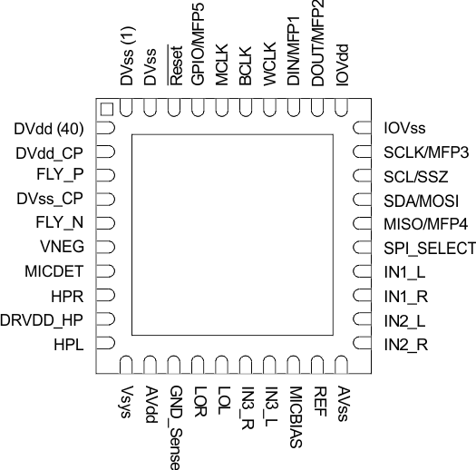
WCSP
(YZF) Package
Bottom View
Pin Functions
| PIN | WCSP (YZF) BALL NO. |
TYPE(1) | DESCRIPTION | ||
|---|---|---|---|---|---|
| NAME | QFN (RSB) NO. | ||||
| DVss | 1 | B2 | GND | Digital ground. Device substrate. | |
| DVss | 2 | A1 | GND | Digital ground | |
| RESET | 3 | C5 | DI | Hardware reset | |
| GPIO | 4 | B3 | DI/O | Primary function: | |
| General purpose digital IO | |||||
| MFP5 | Secondary function: | ||||
| CLKOUT output INT1 output INT2 output Audio serial data bus ADC word clock output Audio serial data bus (secondary) bit clock output Audio serial data bus (secondary) word clock output Digital microphone clock output |
|||||
| MCLK | 5 | A2 | DI | Master clock input | |
| BCLK | 6 | B4 | DI/O | Audio serial data bus (primary) bit clock | |
| WCLK | 7 | A3 | DI/O | Audio serial data bus (primary) word clock | |
| DIN | 8 | A5 | DI | Primary function: | |
| Audio serial data bus data input | |||||
| MFP1 | Secondary function: | ||||
| Digital Microphone Input General Purpose Clock Input General Purpose Input |
|||||
| DOUT | 9 | A4 | DO | Primary function: | |
| Audio serial data bus data output | |||||
| MFP2 | Secondary function: | ||||
| General purpose output Clock output INT1 output INT2 output Audio serial data bus (secondary) bit clock output Audio serial data bus (secondary) word clock output |
|||||
| IOVdd | 10 | A6 | PWR | Supply for IO buffers. 1.1V to 3.6V | |
| IOVss | 11 | B5 | GND | Ground for IO buffers. | |
| SCLK | 12 | C4 | DI | Primary function: (SPI_Select = 1) | |
| SPI serial clock | |||||
| MFP3 | Secondary function:: (SPI_Select = 0) | ||||
| Digital microphone input Audio serial data bus (secondary) bit clock input Audio serial data bus (secondary) DAC/common word clock input Audio serial data bus (secondary) ADC word clock input Audio serial data bus (secondary) data input General purpose input |
|||||
| SCL SS |
13 | B6 | DI | I2C interface serial clock (SPI_Select = 0) SPI interface mode chip-select signal (SPI_Select = 1) |
|
| SDA MOSI |
14 | C3 | DI/O | I2C interface mode serial data input (SPI_Select = 0) SPI interface mode serial data input (SPI_Select = 1) |
|
| MISO | 15 | D4 | DO | Primary function: (SPI_Select = 1) | |
| Serial data output | |||||
| MFP4 | Secondary function: (SPI_Select = 0) | ||||
| General purpose output CLKOUT output INT1 output INT2 output Audio serial data bus (primary) ADC word clock output Digital microphone clock output Audio serial data bus (secondary) data output Audio serial data bus (secondary) bit clock output Audio serial data bus (secondary) word clock output |
|||||
| SPI_SELECT | 16 | C6 | DI | Control mode select pin ( 1 = SPI, 0 = I2C ) | |
| IN1_L | 17 | D6 | AI | Multifunction analog input, Single-ended configuration: MIC 1 or Line 1 left Differential configuration: MIC or Line right, negative |
|
| IN1_R | 18 | E6 | AI | Multifunction analog input, Single-ended configuration: MIC 1 or Line 1 right Differential configuration: MIC or Line right, positive |
|
| IN2_L | 19 | F6 | AI | Multifunction analog input, Single-ended configuration: MIC 2 or Line 2 right Differential configuration: MIC or Line left, positive |
|
| IN2_R | 20 | G6 | AI | Multifunction analog input, Single-ended configuration: MIC 2 or Line 2 right Differential configuration: MIC or Line left, negative |
|
| AVss | 21 | E4, E5 | GND | Analog Ground | |
| REF | 22 | G5 | AO | Reference voltage output for filtering | |
| MICBIAS | 23 | G4 | AO | Microphone bias voltage output | |
| IN3_L | 24 | F5 | AI | Multifunction analog input, Single-ended configuration: MIC3 or Line 3 left, Differential configuration: MIC or Line left, positive, Differential configuration: MIC or Line right, negative |
|
| IN3_R | 25 | F4 | AI | Multifunction analog input, Single-ended configuration: MIC3 or Line 3 right, Differential configuration: MIC or Line left, negative, Differential configuration: MIC or Line right, positive |
|
| LOL | 26 | G3 | AO | Left line output | |
| LOR | 27 | F3 | AO | Right line output | |
| GND_SENSE | 28 | E3 | AI | External ground reference for headphone interface –0.5V to 0.5V | |
| AVdd | 29 | G2 | PWR | Analog voltage supply 1.5V–1.95V | |
| Vsys | 30 | G1 | PWR | Power supply 1.5V–5.5V, Vsys must always be greater than or equal to AVdd and DVdd (Vsys ≥ AVdd, DVdd) | |
| HPL | 31 | F1 | AO | Left headphone output | |
| DRVdd_HP | 32 | F2 | PWR | Power supply for headphone output stage Ground-centered circuit configuration, 1.5V to 1.95V Unipolar circuit configuration, 1.5V to 3.6V |
|
| HPR | 33 | E1 | AO | Right headphone output | |
| MICDET | 34 | E2 | AI | Microphone detection | |
| VNEG | 35 | D1 | PWR | Negative supply for headphones. –1.8V to 0V Input when charge pump is disabled, Filtering output when charge pump is enabled |
|
| FLY_N | 36 | D2 | PWR | Negative terminal for charge-pump flying capacitor | |
| DVss_CP | 37 | D3 | GND | Charge pump ground | |
| FLY_P | 38 | C2 | PWR | Positive terminal for charge pump flying capacitor | |
| DVdd_CP | 39 | C1 | PWR | Charge Pump supply; recommended to connect to DVdd | |
| DVdd | 40 | B1 | PWR | Digital voltage supply 1.26V – 1.95V | |
| Thermal Pad | Thermal Pad | N/A | N/A | Connect to PCB ground plane. Not internally connected. | |