SLOS654D August 2009 – December 2016 TPA3112D1
PRODUCTION DATA.
- 1 Features
- 2 Applications
- 3 Description
- 4 Revision History
- 5 Pin Configuration and Functions
- 6 Specifications
- 7 Detailed Description
-
8 Application and Implementation
- 8.1 Application Information
- 8.2
Typical Application
- 8.2.1 Design Requirements
- 8.2.2
Detailed Design Procedure
- 8.2.2.1 Ferrite Bead Filter Considerations
- 8.2.2.2 Efficiency: LC Filter Required With the Traditional Class-D Modulation Scheme
- 8.2.2.3 When to Use an Output Filter for EMI Suppression
- 8.2.2.4 Input Resistance
- 8.2.2.5 Input Capacitor, CI
- 8.2.2.6 BSN and BSP Capacitors
- 8.2.2.7 Differential Inputs
- 8.2.2.8 Using Low-ESR Capacitors
- 8.2.3 Application Curves
- 9 Power Supply Recommendations
- 10Layout
- 11Device and Documentation Support
- 12Mechanical, Packaging, and Orderable Information
6 Specifications
6.1 Absolute Maximum Ratings
over operating free-air temperature range (unless otherwise noted)(1)
(1) Stresses beyond those listed under absolute maximum ratings may cause permanent damage to the device. These are stress ratings only, and functional operations of the device at these or any other conditions beyond those indicated under recommended operating conditions is not implied. Exposure to absolute-maximum-rated conditions for extended periods may affect device reliability.
6.2 ESD Ratings
| VALUE | UNIT | |||
|---|---|---|---|---|
| V(ESD) | Electrostatic discharge | Human-body model (HBM), per ANSI/ESDA/JEDEC JS-001(1) | ±2000 | V |
| Charged-device model (CDM), per JEDEC specification JESD22-C101(2) | ±500 | |||
(1) JEDEC document JEP155 states that 500-V HBM allows safe manufacturing with a standard ESD control process.
(2) JEDEC document JEP157 states that 250-V CDM allows safe manufacturing with a standard ESD control process.
6.3 Recommended Operating Conditions
over operating free-air temperature range (unless otherwise noted)| MIN | NOM | MAX | UNIT | |||
|---|---|---|---|---|---|---|
| VCC | Supply voltage | PVCC, AVCC | 8 | 26 | V | |
| VIH | High-level input voltage | SD, GAIN0, GAIN1 | 2 | V | ||
| VIL | Low-level input voltage | SD, GAIN0, GAIN1 | 0.8 | V | ||
| VOL | Low-level output voltage | FAULT, RPULLUP = 100 kΩ, VCC = 26 V | 0.8 | V | ||
| IIH | High-level input current | SD, GAIN0, GAIN1, VI = 2 V, VCC = 18 V | 50 | µA | ||
| IIL | Low-level input current | SD, GAIN0, GAIN1, VI = 0.8 V, VCC = 18 V | 5 | µA | ||
6.4 Thermal Information
| THERMAL METRIC(1) | TPA3112D1 | UNIT | |
|---|---|---|---|
| PWP (HTSSOP) | |||
| 28 PINS | |||
| RθJA | Junction-to-ambient thermal resistance | 30.0 | °C/W |
| RθJC(top) | Junction-to-case (top) thermal resistance | 33.5 | °C/W |
| RθJB | Junction-to-board thermal resistance | 17.5 | °C/W |
| ψJT | Junction-to-top characterization parameter | 0.9 | °C/W |
| ψJB | Junction-to-board characterization parameter | 7.2 | °C/W |
| RθJC(bot) | Junction-to-case (bottom) thermal resistance | 0.9 | °C/W |
(1) For more information about traditional and new thermal metrics, see the Semiconductor and IC Package Thermal Metrics application report.
6.5 DC Characteristics, VCC = 24 V
TA = 25°C, RL = 8 Ω (unless otherwise noted)| PARAMETER | TEST CONDITIONS | MIN | TYP | MAX | UNIT | ||
|---|---|---|---|---|---|---|---|
| | VOS | | Class-D output offset voltage (measured differentially) | VI = 0 V, Gain = 36 dB | 1.5 | 15 | mV | ||
| ICC | Quiescent supply current | SD = 2 V, no load, PVcc=21 V | 40 | mA | |||
| ICC(SD) | Quiescent supply current in shutdown mode | SD = 0.8 V, no load, PVcc=21 V | 400 | µA | |||
| rDS(on) | Drain-source on-state resistance | IO = 500 mA, TJ = 25°C |
High side | 240 | mΩ | ||
| Low side | 240 | ||||||
| G | Gain | GAIN1 = 0.8 V | GAIN0 = 0.8 V | 19 | 20 | 21 | dB |
| GAIN0 = 2 V | 25 | 26 | 27 | ||||
| GAIN1 = 2 V | GAIN0 = 0.8 V | 31 | 32 | 33 | dB | ||
| GAIN0 = 2 V | 35 | 36 | 37 | ||||
| tON | Turn-on time | SD = 2 V | 10 | ms | |||
| tOFF | Turn-off time | SD = 0.8 V | 2 | μs | |||
| GVDD | Gate Drive Supply | IGVDD = 2 mA | 6.5 | 6.9 | 7.3 | V | |
6.6 DC Characteristics, VCC = 12 V
TA = 25°C, RL = 8 Ω (unless otherwise noted)| PARAMETER | TEST CONDITIONS | MIN | TYP | MAX | UNIT | ||
|---|---|---|---|---|---|---|---|
| | VOS | | Class-D output offset voltage (measured differentially) | VI = 0 V, Gain = 36 dB | 1.5 | 15 | mV | ||
| ICC | Quiescent supply current | SD = 2 V, no load, PVcc=12 V | 20 | mA | |||
| ICC(SD) | Quiescent supply current in shutdown mode | SD = 0.8 V, no load, PVcc=12 V | 200 | µA | |||
| rDS(on) | Drain-source on-state resistance | IO = 500 mA, TJ = 25°C |
High side | 240 | mΩ | ||
| Low side | 240 | ||||||
| G | Gain | GAIN1 = 0.8 V | GAIN0 = 0.8 V | 19 | 20 | 21 | dB |
| GAIN0 = 2 V | 25 | 26 | 27 | ||||
| GAIN1 = 2 V | GAIN0 = 0.8 V | 31 | 32 | 33 | dB | ||
| GAIN0 = 2 V | 35 | 36 | 37 | ||||
| tON | Turn-on time | SD = 2 V | 10 | ms | |||
| tOFF | Turn-off time | SD = 0.8 V | 2 | μs | |||
| GVDD | Gate Drive Supply | IGVDD = 2 mA | 6.5 | 6.9 | 7.3 | V | |
| PLIMIT | Output Voltage maximum under PLIMIT control | VPLIMIT= 2.0 V; VI= 6.0-V differential | 6.75 | 7.90 | 8.75 | V | |
6.7 AC Characteristics, VCC = 24 V
TA = 25°C, RL = 8 Ω (unless otherwise noted)| PARAMETER | TEST CONDITIONS | MIN | TYP | MAX | UNIT | |
|---|---|---|---|---|---|---|
| KSVR | Power Supply ripple rejection | 200-mVPP ripple from 20 Hz–1 kHz, Gain = 20 dB, Inputs AC-coupled to AGND |
–70 | dB | ||
| PO | Continuous output power | THD+N ≤ 0.1%, f = 1 kHz, VCC = 24 V | 25 | W | ||
| THD+N | Total harmonic distortion + noise | VCC = 24 V, f = 1 kHz, PO = 12 W (half-power) | <0.05% | |||
| Vn | Output integrated noise | 20 Hz to 22 kHz, A-weighted filter, Gain = 20 dB | 65 | µV | ||
| –80 | dBV | |||||
| Crosstalk | VO = 1 Vrms, Gain = 20 dB, f = 1 kHz | –70 | dB | |||
| SNR | Signal-to-noise ratio | Maximum output at THD+N < 1%, f = 1 kHz, Gain = 20 dB, A-weighted |
102 | dB | ||
| fOSC | Oscillator frequency | 250 | 310 | 350 | kHz | |
| Thermal trip point | 150 | °C | ||||
| Thermal hysteresis | 15 | °C | ||||
6.8 AC Characteristics, VCC = 12 V
TA = 25°C, RL = 8 Ω (unless otherwise noted)| PARAMETER | TEST CONDITIONS | MIN | TYP | MAX | UNIT | |
|---|---|---|---|---|---|---|
| KSVR | Supply ripple rejection | 200-mVPP ripple from 20 Hz–1 kHz, Gain = 20 dB, Inputs ac-coupled to AGND |
–70 | dB | ||
| PO | Continuous output power | THD+N ≤ 10%, f = 1 kHz , RL = 8 Ω | 10 | W | ||
| PO | Continuous output power | THD+N ≤ 10%, f = 1 kHz , RL = 4 Ω | 20 | W | ||
| THD+N | Total harmonic distortion + noise | RL = 8 Ω, f = 1 kHz, PO = 5 W (half-power) | <0.06% | |||
| Vn | Output integrated noise | 20 Hz to 22 kHz, A-weighted filter, Gain = 20 dB | 65 | µV | ||
| –80 | dBV | |||||
| Crosstalk | Po = 1 W, Gain = 20 dB, f = 1 kHz | –70 | dB | |||
| SNR | Signal-to-noise ratio | Maximum output at THD+N < 1%, f = 1 kHz, Gain = 20 dB, A-weighted |
102 | dB | ||
| fOSC | Oscillator frequency | 250 | 310 | 350 | kHz | |
| Thermal trip point | 150 | °C | ||||
| Thermal hysteresis | 15 | °C | ||||
6.9 Typical Characteristics
(All Measurements taken at 1 kHz, unless otherwise noted. Measurements were made using the TPA3112D2 EVM which is available at ti.com.)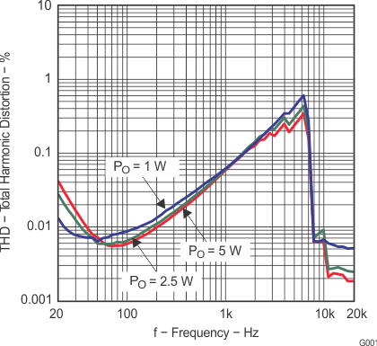
| Gain = 20 dB | VCC = 12 V | ZL = 8 Ω + 66 µH |
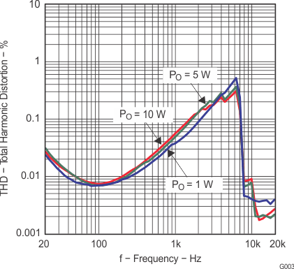
| Gain = 20 dB | VCC = 12 V | ZL = 4 Ω + 33 µH |
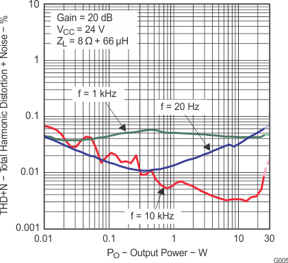
Note: Dashed lines represent thermally limited region.
| Gain = 20 dB | VCC = 24 V | ZL = 8 Ω + 66 µH |
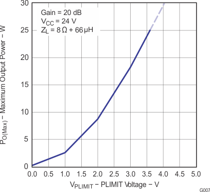
Note: Dashed line represents thermally limited region.
| Gain = 20 dB | VCC = 24 V | ZL = 8 Ω + 66 µH |
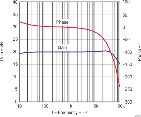
| Gain = 20 dB | VCC = 12 V | ZL = 8 Ω + 66 µH |
| CI = µF | VI = 0.1 VRMS |
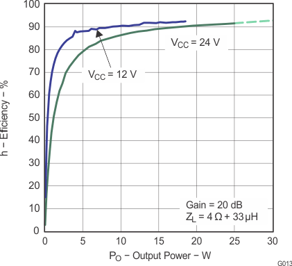
Note: Dashed line represents thermally limited region.
| Gain = 20 dB | ZL = 4 Ω + 33 µH |
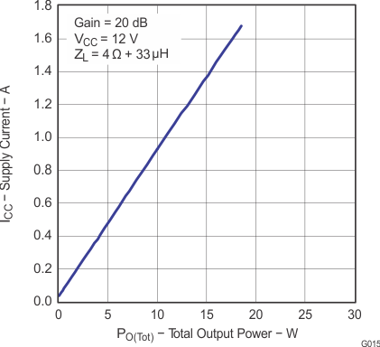
| Gain = 20 dB | VCC = 12 V | ZL = 4 Ω + 33 µH |
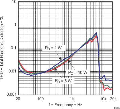
| Gain = 20 dB | VCC = 24 V | ZL = 8 Ω + 66 µH |
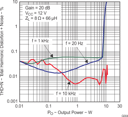
| Gain = 20 dB | VCC = 12 V | ZL = 8 Ω + 66 µH |
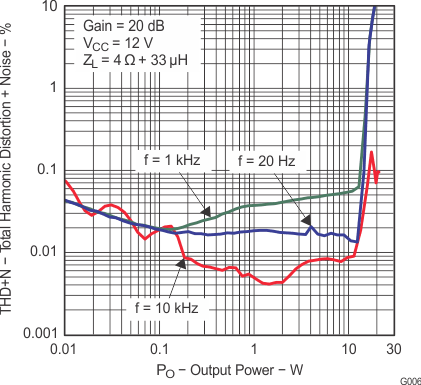
| Gain = 20 dB | VCC = 12 V | ZL = 4 Ω + 33 µH |
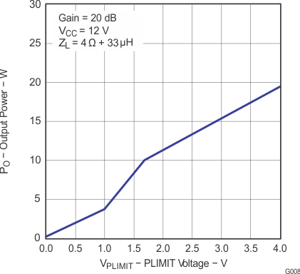
| Gain = 20 dB | VCC = 12 V | ZL = 4 Ω + 33 µH |
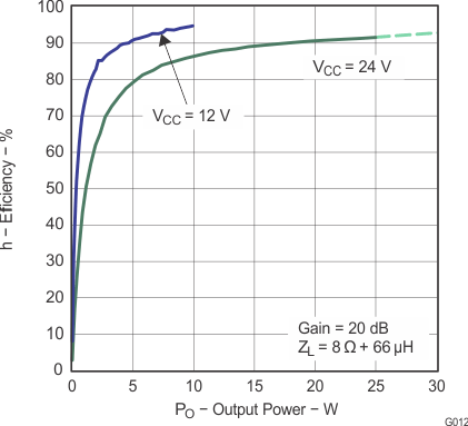
Note: Dashed line represents thermally limited region.
| Gain = 20 dB | ZL = 8 Ω + 66 µH |
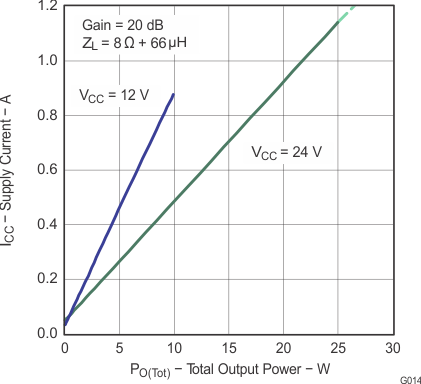
Note: Dashed line represents thermally limited region.
| Gain = 20 dB | ZL = 8 Ω + 66 µH |
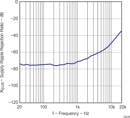
| Gain = 20 dB | VCC = 12 V | ZL = 8 Ω + 66 µH |