SLOS700C January 2011 – April 2016 TPA6139A2
UNLESS OTHERWISE NOTED, this document contains PRODUCTION DATA.
- 1 Features
- 2 Applications
- 3 Description
- 4 Revision History
- 5 Device Comparison Table
- 6 Pin Configuration and Functions
- 7 Specifications
- 8 Parameter Measurement Information
- 9 Detailed Description
- 10Application and Implementation
- 11Power Supply Recommendations
- 12Layout
- 13Device and Documentation Support
- 14Mechanical, Packaging, and Orderable Information
9 Detailed Description
9.1 Overview
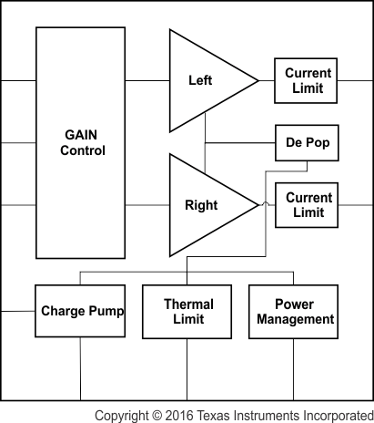
The TPA6139A2 is a DirectPath stereo headphone amplifier that requires no output DC-blocking capacitors and is capable of delivering 25 mW into a 32-Ω load. The device has built-in pop suppression circuitry to completely eliminate pop noise during turnon and turnoff. The amplifier outputs have short-circuit protection.
The TPA6139A2 gain is controlled by external resistors Rin and Rfb, see Gain Setting for recommended values.
The TPA6139A2 operates from a single 3-V to 3.6-V supply, as it uses a built-in charge pump to generate a negative voltage supply for the headphone amplifiers.
9.2 Functional Block Diagram

9.3 Feature Description
9.3.1 DirectPath Headphone Driver
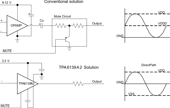
Single-supply line-driver amplifiers typically require DC-blocking capacitors. The top drawing in Figure 9 illustrates the conventional line-driver amplifier connection to the load and output signal.
DC-blocking capacitors are often large in value, and a mute circuit is needed during power up to minimize click and pop. The output capacitor and mute circuit consume PCB area and increase cost of assembly, and can reduce the fidelity of the audio output signal.
 Figure 9. Conventional and DirectPath Line Driver
The DirectPath amplifier architecture operates from a single supply but makes use of an internal charge pump to provide a negative voltage rail.
Combining the user-provided positive rail and the negative rail generated by the IC, the device operates in what is effectively a split supply mode.
The output voltages are now centered at zero volts with the capability to swing to the positive rail or negative rail. Combining this with the built-in click and pop reduction circuit, the DirectPath amplifier requires no output DC-blocking capacitors.
The bottom block diagram and waveform of Figure 9 illustrate the ground-referenced line-driver architecture.
9.4 Device Functional Modes
9.4.1 Internal Undervoltage Detection
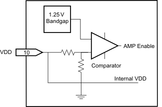
The TPA6139A2 contains an internal precision band-gap reference voltage and a comparator used to monitor the supply voltage, VDD. The internal VDD monitor is set at 2.8 V with 200-mV hysteresis.

9.4.2 Pop-Free Power Up
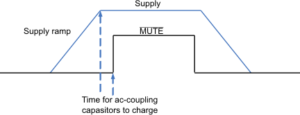
Pop-free power up is ensured by keeping the MUTE low during power-supply ramp-up and ramp-down. The pin must be kept low until the input AC-coupling capacitors are fully charged before asserting the MUTE pin high to precharge the AC-coupling; and, pop-less power up is achieved. Figure 10 illustrates the preferred sequence.
 Figure 10. Power-Up Sequence