-
TAS5721 Digital Audio Power Amplifier With EQ, DRC, 2.1 Support, and Headphone/Line Driver
- 1 Features
- 2 Applications
- 3 Description
- 4 Revision History
- 5 Device Comparison Table
- 6 Pin Configuration and Functions
-
7 Specifications
- 7.1 Absolute Maximum Ratings
- 7.2 ESD Ratings
- 7.3 Recommended Operating Conditions
- 7.4 Thermal Information
- 7.5 Electrical Characteristics - I/O Pin Characteristics
- 7.6 Master Clock Characteristics
- 7.7 Speaker Amplifier Characteristics
- 7.8 Headphone Amplifier and Line Driver Characteristics
- 7.9 Protection Characteristics
- 7.10 I2C Serial Control Port Requirements and Specifications
- 7.11 Serial Audio Port Timing
- 7.12 Typical Characteristics
- 8 Parameter Measurement Information
-
9 Detailed Description
- 9.1 Overview
- 9.2 Functional Block Diagram
- 9.3
Feature Description
- 9.3.1 Power Supply
- 9.3.2 I2C Address Selection and Fault Output
- 9.3.3 Device Protection System
- 9.3.4 Clock, Auto Detection, and PLL
- 9.3.5 PWM Section
- 9.3.6 SSTIMER Functionality
- 9.3.7 2.1-Mode Support
- 9.3.8 PBTL-Mode Support
- 9.3.9 I2C Serial Control Interface
- 9.3.10 Dynamic Range Control (DRC)
- 9.3.11 Bank Switching
- 9.3.12 Serial Data Interface
- 9.3.13 DirectPath Headphone/Line Driver
- 9.4 Device Functional Modes
- 9.5 Programming
- 9.6
Register Maps
- 9.6.1 Clock Control Register (0x00)
- 9.6.2 Device ID Register (0x01)
- 9.6.3 Error Status Register (0x02)
- 9.6.4 System Control Register 1 (0x03)
- 9.6.5 Serial Data Interface Register (0x04)
- 9.6.6 System Control Register 2 (0x05)
- 9.6.7 Soft Mute Register (0x06)
- 9.6.8 Volume Registers (0x07, 0x08, 0x09, 0x0A)
- 9.6.9 Volume Configuration Register (0x0E)
- 9.6.10 Modulation Limit Register (0x10)
- 9.6.11 Interchannel Delay Registers (0x11, 0x12, 0x13, and 0x14)
- 9.6.12 Pwm Shutdown Group Register (0x19)
- 9.6.13 Start/stop Period Register (0x1A)
- 9.6.14 Oscillator Trim Register (0x1B)
- 9.6.15 BKND_ERR Register (0x1C)
- 9.6.16 Input Multiplexer Register (0x20)
- 9.6.17 Channel 4 Source Select Register (0x21)
- 9.6.18 PWM Output MUX Register (0x25)
- 9.6.19 DRC Control (0x46)
- 9.6.20 Bank Switch and EQ Control (0x50)
-
10Application and Implementation
- 10.1 Application Information
- 10.2 Typical Application
- 10.3 System Examples
- 11Power Supply Recommendations
- 12Layout
- 13Device and Documentation Support
- 14Mechanical, Packaging, and Orderable Information
- IMPORTANT NOTICE
TAS5721 Digital Audio Power Amplifier With EQ, DRC, 2.1 Support, and Headphone/Line Driver
1 Features
-
Audio Input/Output
- 10 W x 2 into 8 Ω With PVDD = 24 V
- 8 W x 2 + 12 W x 1 into 8 Ω With PVDD = 24 V
- Supports 2.0, Single Device 2.1, and Mono Modes
- Supports 8-kHz to 48-kHz Sample Rate (LJ/RJ/I2S)
- Integrated DirectPath™ Headphone Amplifier and 2 VRMS Line Driver
- Audio/PWM Processing
- Independent Channel Volume Controls With 24-dB to Mute in 0.5 dB Steps
- Separate Dynamic Range Control for Satellite and Sub Channels
- 21 Programmable Biquads for Speaker EQ
- Programmable Two-Band Dynamic Range Control
- Support for 3D Effects
- General Features
- I2C™ Serial Control Interface Operational Without MCLK
- Configurable I2C Address (0x34 or 0x36)
- Automatic Sample Rate Detection
- Thermal and Short-Circuit Protection
- Wide PVDD Supply Range (4.5 V to 24 V)
2 Applications
LED/LCD TVs, Soundbar, Docking Stations, PC Speakers
3 Description
The TAS5721 is an efficient, digital-input audio amplifier for driving 2.0 speaker systems configured as a bridge tied load (BTL), 2.1 systems with two satellite speakers and one subwoofer, or in PBTL systems driving a single speaker configured as a parallel bridge tied load (PBTL). One serial data input allows processing of up to two discrete audio channels and seamless integration to most digital audio processors and MPEG decoders. The device accepts a wide range of input data formats and sample rates. A fully programmable data path routes these channels to the internal speaker drivers.
The TAS5721 is a slave-only device, receiving all clocks from external sources. The TAS5721 operates with a PWM carrier frequency between a 384-kHz switching rate and a 288-KHz switching rate, depending on the input sample rate. Oversampling, combined with a fourth-order noise shaper, provides a flat noise floor and excellent dynamic range from 20 Hz to 20 kHz.
An integrated ground centered DirectPath™ combination headphone amplifier and 2VRMS line driver is integrated in the TAS5721.
Device Information(1)
| PART NUMBER | PACKAGE | BODY SIZE (NOM) |
|---|---|---|
| TAS5721 | HTSSOP (48) | 12.50 mm × 6.10 mm |
- For all available packages, see the orderable addendum at the end of the data sheet.
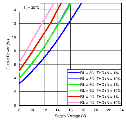
Output Power vs. PVDD in 2.0 Mode

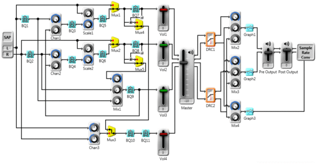
Signal Processing Flow

4 Revision History
Changes from * Revision (July 2012) to A Revision
- Added ESD Ratings table, Feature Description section, Device Functional Modes, Application and Implementation section, Power Supply Recommendations section, Layout section, Device and Documentation Support section, and Mechanical, Packaging, and Orderable Information section.Go