SLOS739A July 2012 – March 2016 TAS5721
PRODUCTION DATA.
- 1 Features
- 2 Applications
- 3 Description
- 4 Revision History
- 5 Device Comparison Table
- 6 Pin Configuration and Functions
-
7 Specifications
- 7.1 Absolute Maximum Ratings
- 7.2 ESD Ratings
- 7.3 Recommended Operating Conditions
- 7.4 Thermal Information
- 7.5 Electrical Characteristics - I/O Pin Characteristics
- 7.6 Master Clock Characteristics
- 7.7 Speaker Amplifier Characteristics
- 7.8 Headphone Amplifier and Line Driver Characteristics
- 7.9 Protection Characteristics
- 7.10 I2C Serial Control Port Requirements and Specifications
- 7.11 Serial Audio Port Timing
- 7.12 Typical Characteristics
- 8 Parameter Measurement Information
-
9 Detailed Description
- 9.1 Overview
- 9.2 Functional Block Diagram
- 9.3
Feature Description
- 9.3.1 Power Supply
- 9.3.2 I2C Address Selection and Fault Output
- 9.3.3 Device Protection System
- 9.3.4 Clock, Auto Detection, and PLL
- 9.3.5 PWM Section
- 9.3.6 SSTIMER Functionality
- 9.3.7 2.1-Mode Support
- 9.3.8 PBTL-Mode Support
- 9.3.9 I2C Serial Control Interface
- 9.3.10 Dynamic Range Control (DRC)
- 9.3.11 Bank Switching
- 9.3.12 Serial Data Interface
- 9.3.13 DirectPath Headphone/Line Driver
- 9.4 Device Functional Modes
- 9.5 Programming
- 9.6
Register Maps
- 9.6.1 Clock Control Register (0x00)
- 9.6.2 Device ID Register (0x01)
- 9.6.3 Error Status Register (0x02)
- 9.6.4 System Control Register 1 (0x03)
- 9.6.5 Serial Data Interface Register (0x04)
- 9.6.6 System Control Register 2 (0x05)
- 9.6.7 Soft Mute Register (0x06)
- 9.6.8 Volume Registers (0x07, 0x08, 0x09, 0x0A)
- 9.6.9 Volume Configuration Register (0x0E)
- 9.6.10 Modulation Limit Register (0x10)
- 9.6.11 Interchannel Delay Registers (0x11, 0x12, 0x13, and 0x14)
- 9.6.12 Pwm Shutdown Group Register (0x19)
- 9.6.13 Start/stop Period Register (0x1A)
- 9.6.14 Oscillator Trim Register (0x1B)
- 9.6.15 BKND_ERR Register (0x1C)
- 9.6.16 Input Multiplexer Register (0x20)
- 9.6.17 Channel 4 Source Select Register (0x21)
- 9.6.18 PWM Output MUX Register (0x25)
- 9.6.19 DRC Control (0x46)
- 9.6.20 Bank Switch and EQ Control (0x50)
-
10Application and Implementation
- 10.1 Application Information
- 10.2 Typical Application
- 10.3 System Examples
- 11Power Supply Recommendations
- 12Layout
- 13Device and Documentation Support
- 14Mechanical, Packaging, and Orderable Information
10 Application and Implementation
NOTE
Information in the following applications sections is not part of the TI component specification, and TI does not warrant its accuracy or completeness. TI’s customers are responsible for determining suitability of components for their purposes. Customers should validate and test their design implementation to confirm system functionality.
10.1 Application Information
The typical connection diagram highlights the required external components and system level connections for proper operation of the device in several popular system examples.
Each of these configurations can be realized using the Evaluation Module (EVM) for the device. These flexible modules allow full evaluation of the device in the most common modes of operation. Any design variation can be supported by TI through schematic and layout reviews. Visit http://e2e.ti.com for design assistance and join the audio amplifier discussion forum for additional information.
10.2 Typical Application
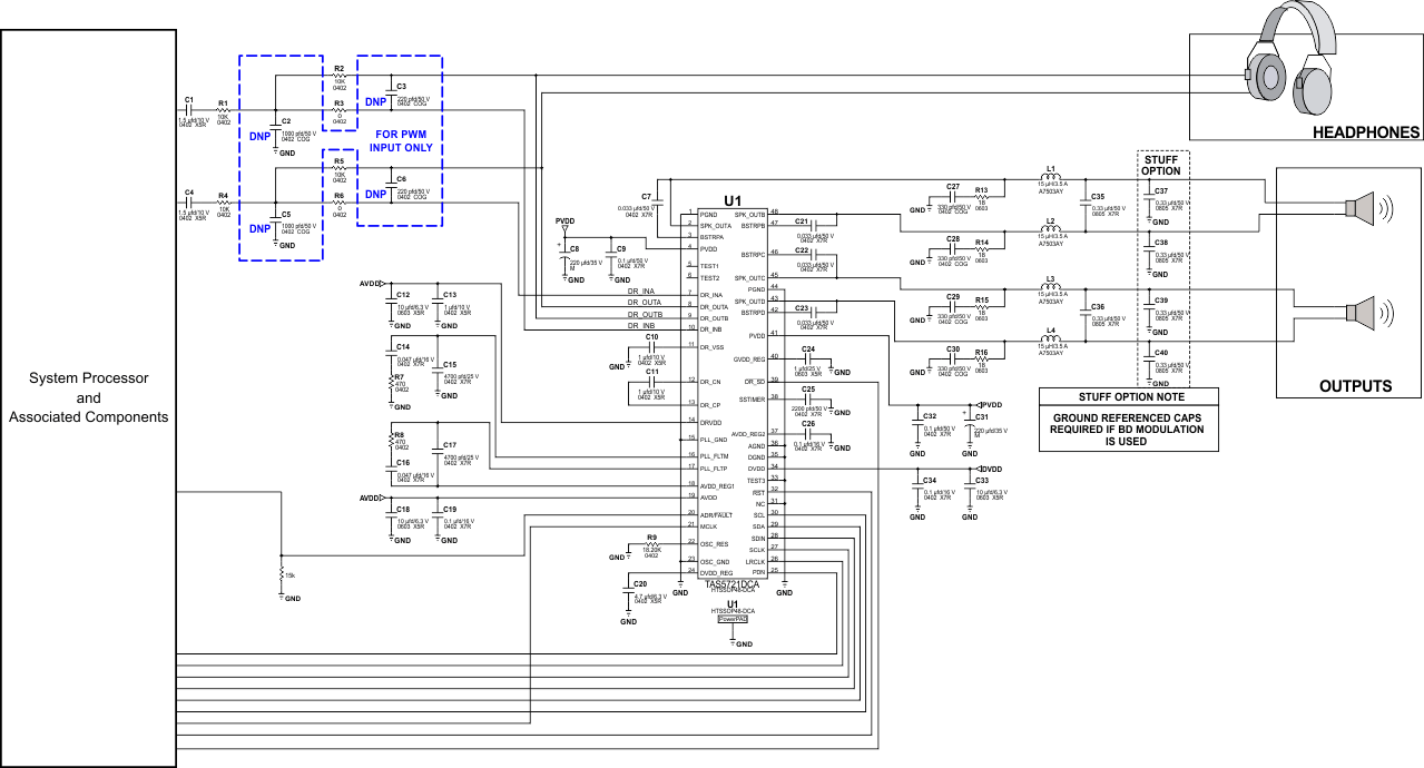 Figure 71. Mono PBTL System With Headphone Driver
10.2.1 Design Requirements
Table 25 lists the design parameters of the TAS5721.
Table 25. Design Parameters
| PARAMETER | EXAMPLE |
|---|---|
| Low Power Supply | 3.3 V |
| High Power Supply | 8 V to 24 V |
| Host Processor | I2S Compliant Master |
| I2C Compliant Master | |
| GPIO Control | |
| Output Filters | Inductor-Capacitor Low Pass Filter(1) |
| Speaker | 8 Ω minimum BTL 4 Ω minimum PBTL and Single Ended |
10.2.2 Detailed Design Procedure
10.2.2.1 Component Selection and Hardware Connections
The typical connections required for proper operation of the device can be found on the TAS5721EVM User’s Guide (SLOU346). The device was tested this this list of components, deviation from this typical application components unless recommended by this document may produce unwanted results, which could range from degradation of audio performance to destructive failure of the device. The application report SLOA119 offers a detailed description on proper component selection and design of the output filter based upon the modulation used, desired load and response.
10.2.2.2 I2C Pullup Resistors
Customary pullup resistors are required on the SCL and SDA signal lines. They are not shown in the Typical Application Circuits, because they are shared by all of the devices on the I²C bus and are considered to be part of the associated passive components for the System Processor. These resistor values should be chosen per the guidance provided in the I²C Specification.
10.2.2.3 Digital I/O Connectivity
The digital I/O lines of the TAS5721 are described in previous sections. As discussed, whenever a static digital pin (that is a pin that is hardwired to be HIGH or LOW) is required to be pulled HIGH, it should be connected to DVDD through a pullup resistor to control the slew rate of the voltage presented to the digital I/O pins. It is not, however, necessary to have a separate pullup resistor for each static digital I/O line. Instead, a single resistor can be used to tie all static I/O lines HIGH to reduce BOM count.
10.2.2.4 Recommended Startup and Shutdown Procedures
10.2.2.4.1 Recommended Use Model
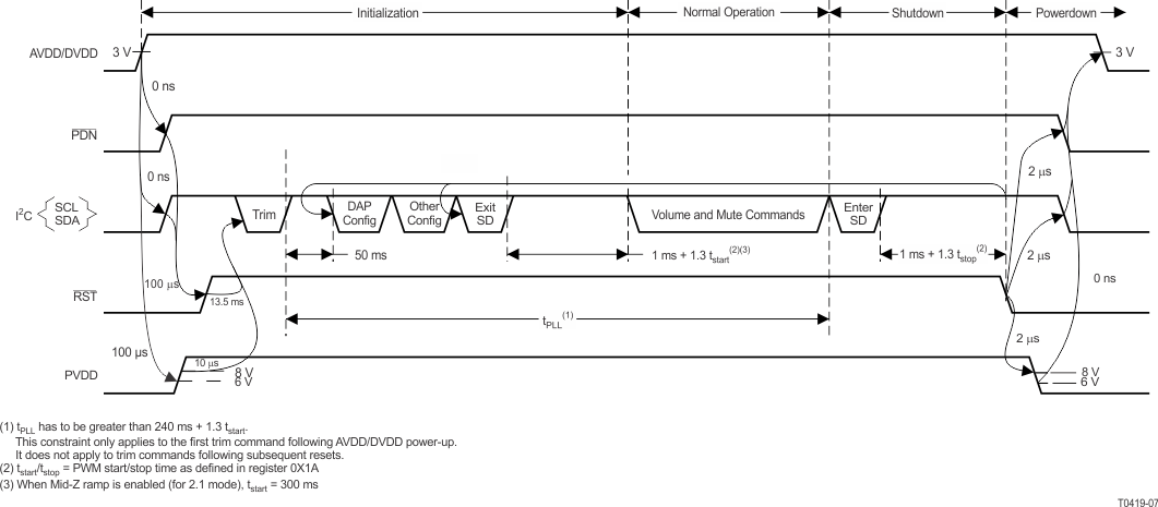 Figure 72. Recommended Command Sequence
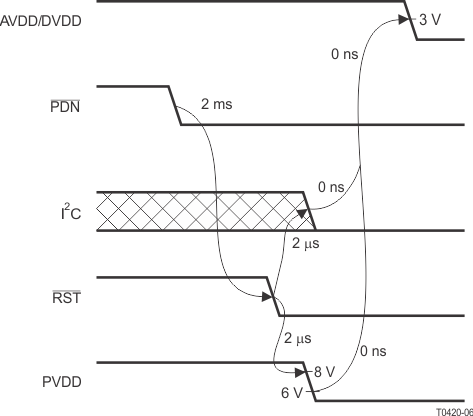 Figure 73. Power Loss Sequence
10.2.2.4.1.1 Initialization Sequence
Use the following sequence to power-up and initialize the device:
- Hold all digital inputs low and ramp up AVDD/DVDD to at least 3 V.
- Initialize digital inputs and PVDD supply as follows:
- Drive RST = 0, PDN = 1, and other digital inputs to their desired state while ensuring that all are never more than 2.5 V above AVDD/DVDD. Wait at least 100 µs, drive RST = 1, and wait at least another 13.5 ms.
- Ramp up PVDD to at least 8 V while ensuring that it remains below 6 V for at least 100 µs after AVDD/DVDD reaches 3 V. Then wait at least another 10 µs.
- Trim oscillator (write 0x00 to register 0x1B) and wait at least 50 ms.
- Configure the DAP via I2C (see Users's Guide for typical values).
- Configure remaining registers.
- Exit shutdown (sequence defined below).
10.2.2.4.1.2 Normal Operation
The following are the only events supported during normal operation:
- Writes to master/channel volume registers.
- Writes to soft mute register.
- Enter and exit shutdown (sequence defined below).
NOTE
Event 3 is not supported for 240 ms + 1.3 × tstart after trim following AVDD/DVDD powerup ramp (where tstart is 300 ms when mid-Z ramp is enabled and is otherwise specified by register 0x1A).
10.2.2.4.1.3 Shutdown Sequence
Enter:
- Write 0x40 to register 0x05.
- Wait at least 1 ms + 1.3 × tstop (where tstop is specified by register 0x1A).
- If desired, reconfigure by returning to step 4 of initialization sequence.
Exit:
- Write 0x00 to register 0x05 (exit shutdown command may not be serviced for as much as 240 ms after trim following AVDD/DVDD powerup ramp).
- Wait at least 1 ms + 1.3 × tstart (where tstart is 300 ms when mid-Z ramp is enabled and is otherwise specified by register 0x1A).
- Proceed with normal operation.
10.2.2.4.1.4 Power-Down Sequence
Use the following sequence to powerdown the device and its supplies:
- If time permits, enter shutdown (sequence defined above); else, in case of sudden power loss, assert PDN = 0 and wait at least 2 ms.
- Assert RST = 0.
- Drive digital inputs low and ramp down PVDD supply as follows:
- Drive all digital inputs low after RST has been low for at least 2 µs.
- Ramp down PVDD while ensuring that it remains above 8 V until RST has been low for at least 2 µs.
- Ramp down AVDD/DVDD while ensuring that it remains above 3 V until PVDD is below 6 V and that it is never more than 2.5 V below the digital inputs.
10.2.3 Application Curves
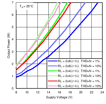 Figure 74. Output Power vs PVDD in 2.1 Mode
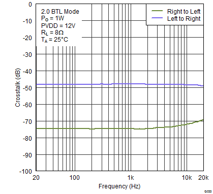 Figure 76. Crosstalk vs Frequency in 2.0 Mode
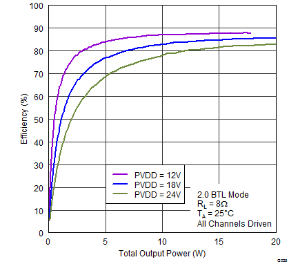 Figure 75. Efficiency vs Output Power in 2.0 Mode
10.3 System Examples
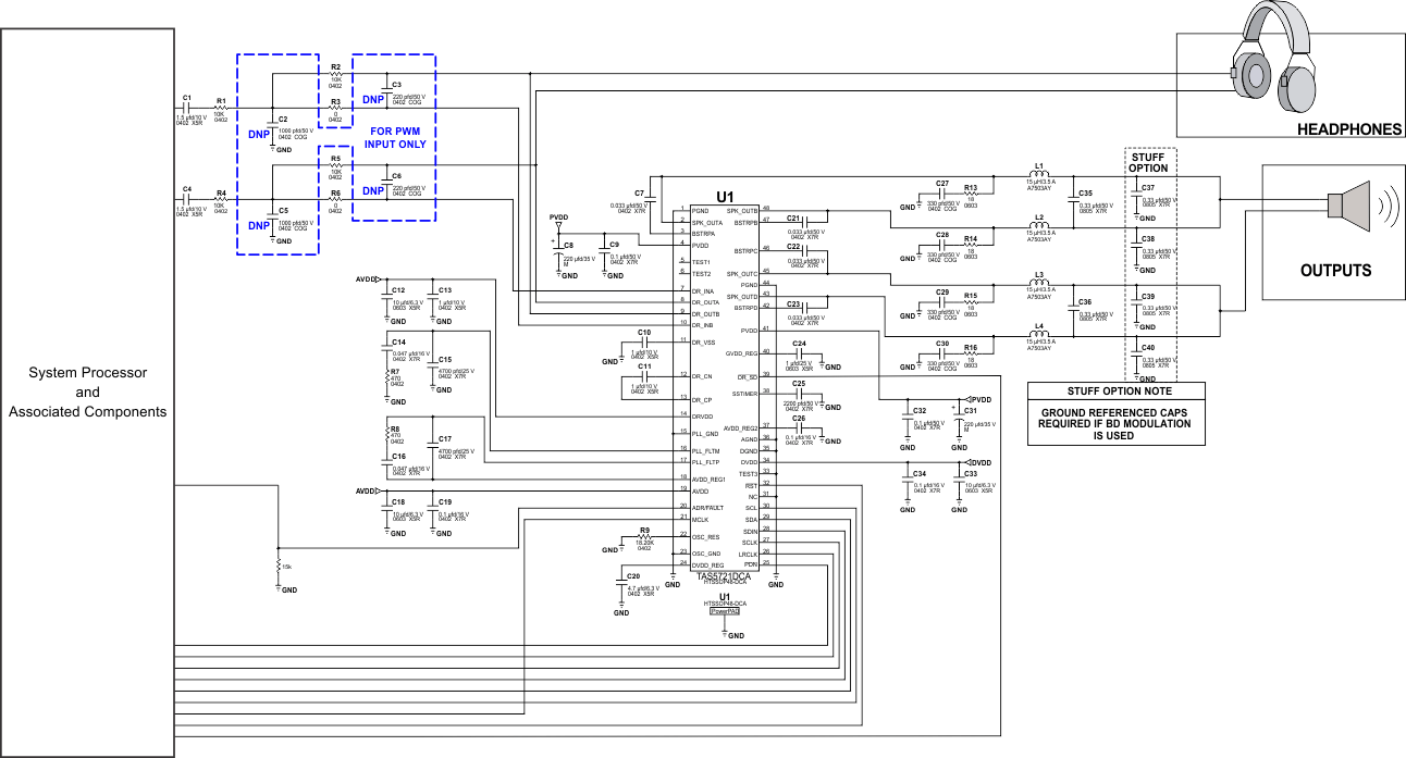 Figure 77. Typical Application Circuit for Stereo (BTL) Configuration
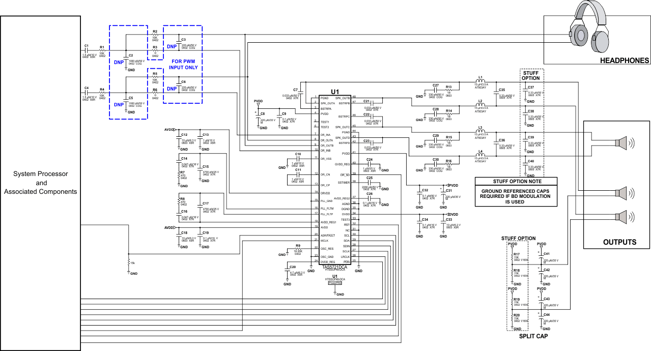 Figure 78. 2.1 System With Headphone Driver
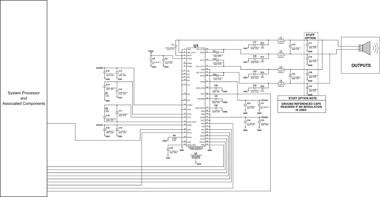 Figure 79. Stereo (BTL) System
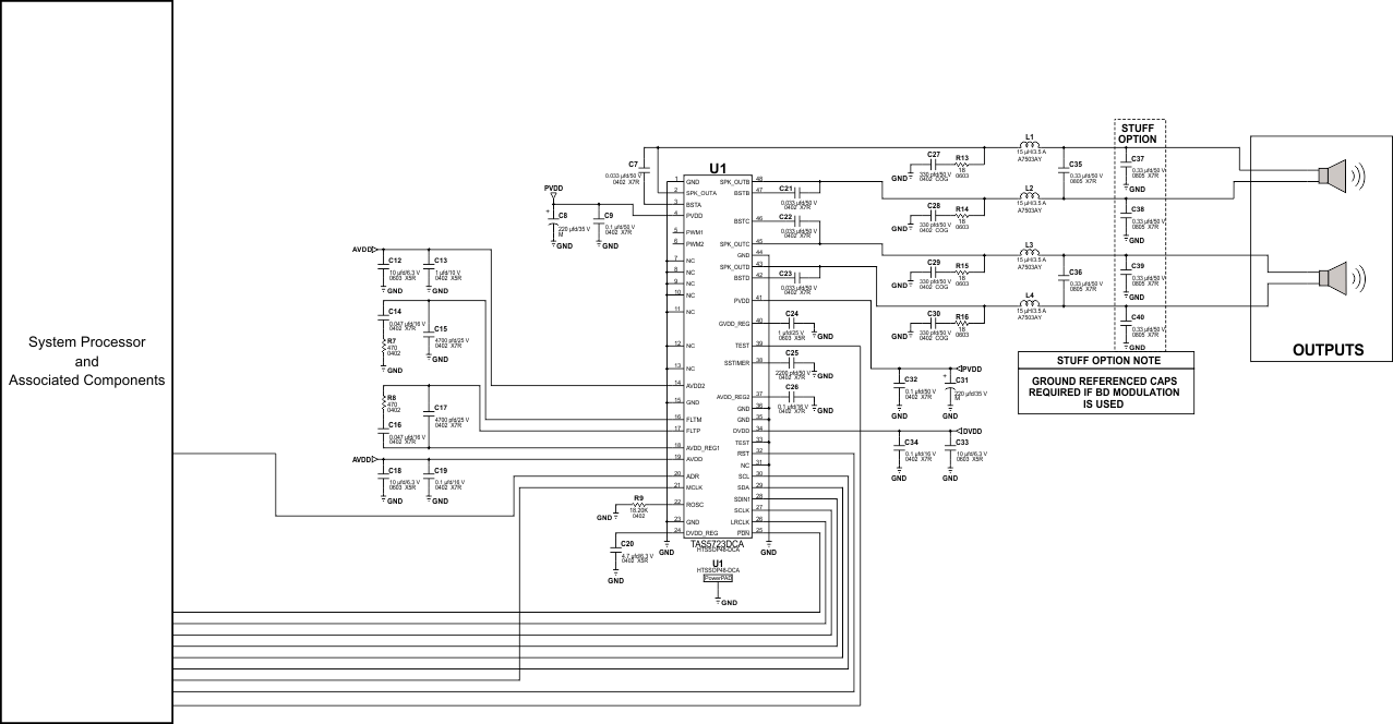 Figure 80. Mono (PBTL) System
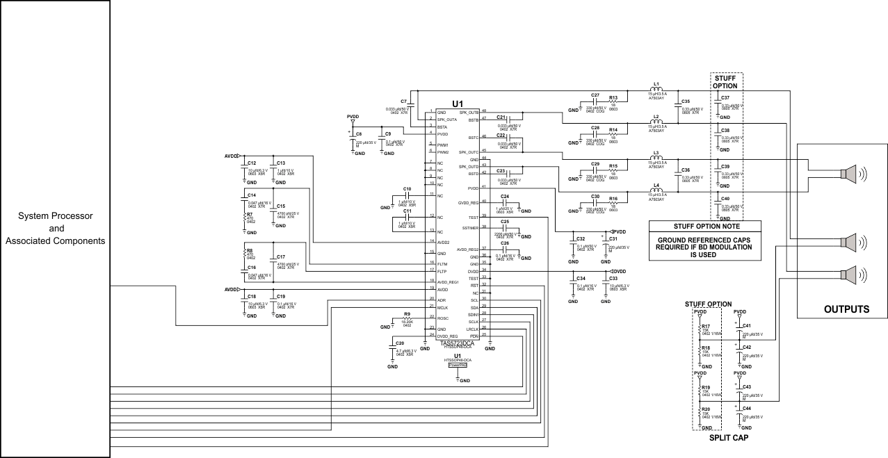 Figure 81. 2.1 System