SLOS741D May 2013 – May 2017 TAS5760MD
PRODUCTION DATA.
- 1 Features
- 2 Applications
- 3 Description
- 4 Revision History
- 5 Device Comparison Table
- 6 Pin Configuration and Functions
-
7 Specifications
- 7.1 Absolute Maximum Ratings
- 7.2 ESD Ratings
- 7.3 Recommended Operating Conditions
- 7.4 Thermal Information
- 7.5 Digital I/O Pins
- 7.6 Master Clock
- 7.7 Serial Audio Port
- 7.8 Protection Circuitry
- 7.9 Speaker Amplifier in All Modes
- 7.10 Speaker Amplifier in Stereo Bridge Tied Load (BTL) Mode
- 7.11 Speaker Amplifier in Mono Parallel Bridge Tied Load (PBTL) Mode
- 7.12 Headphone Amplifier and Line Driver
- 7.13 I²C Control Port
- 7.14 Typical Idle, Mute, Shutdown, Operational Power Consumption
- 7.15 Typical Characteristics (Stereo BTL Mode): fSPK_AMP = 384 kHz
- 7.16 Typical Characteristics (Stereo BTL Mode): fSPK_AMP = 768 kHz
- 7.17 Typical Characteristics (Mono PBTL Mode): fSPK_AMP = 384 kHz
- 7.18 Typical Characteristics (Mono PBTL Mode): fSPK_AMP = 768 kHz
-
8 Detailed Description
- 8.1 Overview
- 8.2 Functional Block Diagram
- 8.3 Feature Description
- 8.4
Device Functional Modes
- 8.4.1
Hardware Control Mode
- 8.4.1.1 Speaker Amplifier Shut Down (SPK_SD Pin)
- 8.4.1.2 Serial Audio Port in Hardware Control Mode
- 8.4.1.3 Soft Clipper Control (SFT_CLIP Pin)
- 8.4.1.4 Speaker Amplifier Switching Frequency Select (FREQ/SDA Pin)
- 8.4.1.5 Parallel Bridge Tied Load Mode Select (PBTL/SCL Pin)
- 8.4.1.6 Speaker Amplifier Sleep Enable (SPK_SLEEP/ADR Pin)
- 8.4.1.7 Speaker Amplifier Gain Select (SPK_GAIN [1:0] Pins)
- 8.4.1.8 Considerations for Setting the Speaker Amplifier Gain Structure
- 8.4.2 Software Control Mode
- 8.4.1
Hardware Control Mode
- 8.5
Register Maps
- 8.5.1 Control Port Registers - Quick Reference
- 8.5.2
Control Port Registers - Detailed Description
- 8.5.2.1 Device Identification Register (0x00)
- 8.5.2.2 Power Control Register (0x01)
- 8.5.2.3 Digital Control Register (0x02)
- 8.5.2.4 Volume Control Configuration Register (0x03)
- 8.5.2.5 Left Channel Volume Control Register (0x04)
- 8.5.2.6 Right Channel Volume Control Register (0x05)
- 8.5.2.7 Analog Control Register (0x06)
- 8.5.2.8 Reserved Register (0x07)
- 8.5.2.9 Fault Configuration and Error Status Register (0x08)
- 8.5.2.10 Reserved Controls (9 / 0x09) - (15 / 0x0F)
- 8.5.2.11 Digital Clipper Control 2 Register (0x10)
- 8.5.2.12 Digital Clipper Control 1 Register (0x11)
-
9 Application and Implementation
- 9.1 Application Information
- 9.2
Typical Applications
- 9.2.1
Stereo BTL Using Software Control
- 9.2.1.1 Design Requirements
- 9.2.1.2
Detailed Design Procedure
- 9.2.1.2.1 Startup Procedures- Software Control Mode
- 9.2.1.2.2 Shutdown Procedures- Software Control Mode
- 9.2.1.2.3 Component Selection and Hardware Connections
- 9.2.1.2.4 Recommended Startup and Shutdown Procedures
- 9.2.1.2.5
Headphone and Line Driver Amplifier
- 9.2.1.2.5.1 Charge-Pump Flying Capacitor and DR_VSS Capacitor
- 9.2.1.2.5.2 Decoupling Capacitors
- 9.2.1.2.5.3 Gain-Setting Resistor Ranges
- 9.2.1.2.5.4 Using the Line Driver Amplifier in the TAS5760MD as a Second-Order Filter
- 9.2.1.2.5.5 External Undervoltage Detection
- 9.2.1.2.5.6 Input-Blocking Capacitors
- 9.2.1.2.6 Gain-Setting Resistors
- 9.2.1.3 Application Curve
- 9.2.2 Stereo BTL Using Hardware Control
- 9.2.3 Mono PBTL Using Software Control
- 9.2.4 Mono PBTL Using Hardware Control
- 9.2.1
Stereo BTL Using Software Control
- 10Power Supply Recommendations
- 11Layout
- 12Device and Documentation Support
- 13Mechanical, Packaging, and Orderable Information
9 Application and Implementation
NOTE
Information in the following applications sections is not part of the TI component specification, and TI does not warrant its accuracy or completeness. TI’s customers are responsible for determining suitability of components for their purposes. Customers should validate and test their design implementation to confirm system functionality.
9.1 Application Information
These typical connection diagrams highlight the required external components and system level connections for proper operation of the device in several popular use cases.
Each of these configurations can be realized using the Evaluation Modules (EVMs) for the device. These flexible modules allow full evaluation of the device in all available modes of operation. Additionally, some of the application circuits are available as reference designs and can be found on the TI website. Also see the TAS5760MD's product page for information on ordering the EVM. Not all configurations are available as reference designs; however, any design variation can be supported by TI through schematic and layout reviews. Visit support.ti.com for additional design assistance. Also, join the audio amplifier discussion forum at http://e2e.ti.com.
9.2 Typical Applications
These application circuits detail the recommended component selection and board configurations for the TAS5760MD device. Note that in Software Control mode, the clipping point of the amplifier and thus the rated power of the end equipment can be set using the digital clipper if desired. Additionally, if the sonic signature of the soft clipper is preferred, it can be used in addition to or in lieu of the digital clipper. The software control application circuit detailed in this section shows the soft clipper in its bypassed state, which results in a lower BOM count than when using the soft clipper. The trade-off between the sonic characteristics of the clipping events in the amplifier and BOM minimization can be chosen based upon the design goals related to the end product.
9.2.1 Stereo BTL Using Software Control
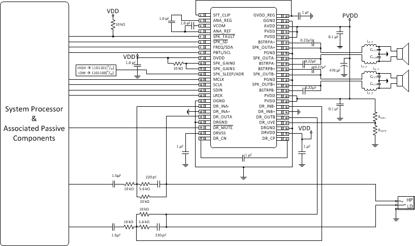 Figure 63. Stereo BTL Using Software Control
9.2.1.1 Design Requirements
For this design example, use the parameters listed in Table 19 as the input parameters.
Table 19. Design Parameters
| PARAMETER | EXAMPLE |
|---|---|
| Low Power Supply | 3.3 V |
| High Power Supply | 5 V to 24 V |
| Host Processor | I2S Compliant Master |
| I2C Compliant Master | |
| GPIO Control | |
| Output Filters | Inductor-Capacitor Low Pass Filter |
| Speakers | 4 Ω to 8 Ω |
9.2.1.2 Detailed Design Procedure
9.2.1.2.1 Startup Procedures- Software Control Mode
- Configure all digital I/O pins as required by the application using PCB connections (that is SPK_GAIN[1:0] = 11, ADR, etc.)
- Start with SPK_SD Pin = LOW
- Bring up power supplies (it does not matter if PVDD/AVDD or DVDD comes up first, provided the device is held in shutdown.)
- Once power supplies are stable, start MCLK, SCLK, LRCK
- Configure the device via the control port in the manner required by the use case, making sure to mute the device via the control port
- Once power supplies and clocks are stable and the control port has been programmed, bring SPK_SD HIGH
- Unmute the device via the control port
- The device is now in normal operation
NOTE
Control port register changes should only occur when the device is placed into shutdown. This can be accomplished either by pulling the SPK_SD pin LOW or clearing the SPK_SD bit in the control port.
9.2.1.2.2 Shutdown Procedures- Software Control Mode
- The device is in normal operation
- Mute via the control port
- Pull SPK_SD LOW
- The clocks can now be stopped and the power supplies brought down
- The device is now fully shutdown and powered off
NOTE
Any control port register changes excluding volume control changes should only occur when the device is placed into shutdown. This can be accomplished either by pulling the SPK_SD pin LOW or clearing the SPK_SD bit in the control port.
9.2.1.2.3 Component Selection and Hardware Connections
Figure 63 details the typical connections required for proper operation of the device. It is with this list of components that the device was simulated, tested, and characterized. Deviation from this typical application circuit unless recommended by this document may produce unwanted results, which could range from degradation of audio performance to destructive failure of the device.
9.2.1.2.3.1 I²C Pullup Resistors
It is important to note that when the device is operated in Software Control Mode, the customary pullup resistors are required on the SCL and SDA signal lines. They are not shown in the Typical Application Circuits, because they are shared by all of the devices on the I²C bus and are considered to be part of the associated passive components for the System Processor. These resistor values should be chosen per the guidance provided in the I²C Specification.
9.2.1.2.3.2 Digital I/O Connectivity
The digital I/O lines of the TAS5760MD are described in previous sections. As discussed, whenever a static digital pin (that is a pin that is hardwired to be HIGH or LOW) is required to be pulled HIGH, it should be connected to DVDD through a pullup resistor to control the slew rate of the voltage presented to the digital I/O pins. It is not, however, necessary to have a separate pullup resistor for each static digital I/O line. Instead, a single resistor can be used to tie all static I/O lines HIGH to reduce BOM count. For instance, if Software Control Mode is desired both the GAIN[1:0] and the PBTL/SCL pins can both be pulled HIGH through a single pullup resistor.
9.2.1.2.4 Recommended Startup and Shutdown Procedures
The start up and shutdown procedures for both Hardware Control Mode and Software Control Mode are shown below.
9.2.1.2.5 Headphone and Line Driver Amplifier
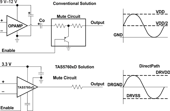
Single-supply line-driver amplifiers typically require dc-blocking capacitors. The top drawing in Figure 64 illustrates the conventional line-driver amplifier connection to the load and output signal. DC blocking capacitors are often large in value. The line load (typical resistive values of 600 Ω to 10 kΩ) combines with the dc blocking capacitors to form a high-pass filter. Equation 3 shows the relationship between the load impedance (RL), the capacitor (CO), and the cutoff frequency (fC).

CO can be determined using Equation 4, where the load impedance and the cutoff frequency are known.

If fC is low, the capacitor must then have a large value because the load resistance is small. Large capacitance values require large package sizes. Large package sizes consume PCB area, stand high above the PCB, increase cost of assembly, and can reduce the fidelity of the audio output signal.
The DirectPath amplifier architecture operates from a single supply but makes use of an internal charge pump to provide a negative voltage rail. Combining the user-provided positive rail and the negative rail generated by the IC, the device operates in what is effectively a split-supply mode. The output voltages are now centered at zero volts with the capability to swing to the positive rail or negative rail. Combining this with the built-in click and pop reduction circuit, the DirectPath amplifier requires no output dc blocking capacitors. The bottom block diagram and waveform of Figure 64 illustrate the ground-referenced line-driver architecture. This is the architecture of the headphone / line driver inside of the TAS5760MD.
9.2.1.2.5.1 Charge-Pump Flying Capacitor and DR_VSS Capacitor
The charge-pump flying capacitor serves to transfer charge during the generation of the negative supply voltage. The PVSS capacitor must be at least equal to the charge-pump capacitor in order to allow maximum charge transfer. Low-ESR capacitors are an ideal selection, and a value of 1 µF is typical. Capacitor values that are smaller than 1 µF can be used, but the maximum output voltage may be reduced and the device may not operate to specifications. If the TAS5760MD is used in highly noise-sensitive circuits, it is recommended to add a small LC filter on the DRVDD connection.
9.2.1.2.5.2 Decoupling Capacitors
The TAS5760MD contains a DirectPath line-driver amplifier that requires adequate power supply decoupling to ensure that the noise and total harmonic distortion (THD) are low. A good, low equivalent-series-resistance (ESR) ceramic capacitor, typically 1 µF, placed as close as possible to the device DRVDD lead works best. Placing this decoupling capacitor close to the TAS5760MD is important for the performance of the amplifier. For filtering lower-frequency noise signals, a 10-µF or greater capacitor placed near the audio power amplifier would also help, but it is not required in most applications because of the high PSRR of this device.
9.2.1.2.5.3 Gain-Setting Resistor Ranges
The gain-setting resistors, RIN and Rfb, must be chosen so that noise, stability, and input capacitor size of the headphone amplifier / line driver inside the TAS5760MD are kept within acceptable limits. Voltage gain is defined as Rfb divided by RIN.
Selecting values that are too low demands a large input ac-coupling capacitor, CIN. Selecting values that are too high increases the noise of the amplifier. Table 20 lists the recommended resistor values for different inverting-input gain settings.
Table 20. Recommended Resistor Values
| GAIN | INPUT RESISTOR VALUE, RIN | FEEDBACK RESISTOR VALUE, Rfb |
|---|---|---|
| –1 V/V | 10 kΩ | 10 kΩ |
| –1.5 V/V | 8.2 kΩ | 12 kΩ |
| –2 V/V | 15 kΩ | 30 kΩ |
| –10 V/V | 4.7 kΩ | 47 kΩ |
9.2.1.2.5.4 Using the Line Driver Amplifier in the TAS5760MD as a Second-Order Filter
Several audio DACs used today require an external low-pass filter to remove out-of-band noise. This is possible with the headphone amplifier / line driver inside the TAS5760MD, as it can be used like a standard operational amplifier. Several filter topologies can be implemented, both single-ended and differential. In Figure 65, multi-feedback (MFB) with differential input and single-ended input are shown.
An ac-coupling capacitor to remove dc content from the source is shown; it serves to block any dc content from the source and lowers the dc gain to 1, helping to reduce the output dc offset to a minimum.
The component values can be calculated with the help of the TI FilterPro™ program available on the TI Web site at: http://focus.ti.com/docs/toolsw/folders/print/filterpro.html.
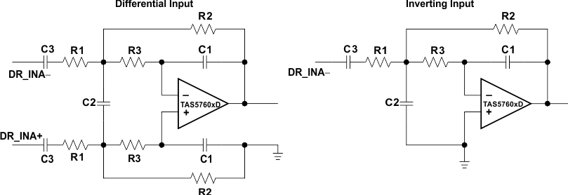 Figure 65. Second-Order Active Low-Pass Filter
The resistor values should have a low value for obtaining low noise, but should also have a high enough value to get a small-size ac-coupling capacitor. With the proposed values of R1 = 15 kΩ, R2 = 30 kΩ, and R3 = 43 kΩ, a dynamic range (DYR) of 106 dB can be achieved with a 1-mF input ac-coupling capacitor.
9.2.1.2.5.5 External Undervoltage Detection
External undervoltage detection can be used to mute/shut down the heaphone / line driver amplifier in the TAS5760MD before an input device can generate a pop. The shutdown threshold at the UVP pin is 1.25 V. The user selects a resistor divider to obtain the shutdown threshold and hysteresis for the specific application. The thresholds can be determined as follows:
For example, to obtain VUVP = 3.8 V and 1-V hysteresis, we can use R1 = 3 kΩ, R2 = 1 kΩ, and R3 = 50 kΩ.
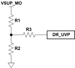 Figure 66. External Undervoltage Detection
9.2.1.2.5.6 Input-Blocking Capacitors
DC input-blocking capacitors are required to be added in series with the audio signal into the input pins of the headphone amplifier / line driver inside the TAS5760MD. These capacitors block the dc portion of the audio source and allow the headphone / line driver amplifier inside the TAS5760MD.
These capacitors form a high-pass filter with the input resistor, RIN. The cutoff frequency is calculated using Equation 7. For this calculation, the capacitance used is the input-blocking capacitor, and the resistance is the input resistor chosen from Table 20; then the frequency and/or capacitance can be determined when one of the two values is given.
It is recommended to use electrolytic capacitors or high-voltage-rated capacitors as input blocking capacitors to ensure minimal variation in capacitance with input voltages. Such variation in capacitance with input voltages is commonly seen in ceramic capacitors and can increase low-frequency audio distortion.

9.2.1.2.6 Gain-Setting Resistors
The gain-setting resistors, RIN and Rfb, must be placed close to their respective pins to minimize capacitive loading on these input pins and to ensure maximum stability of the headphone / line driver inside the TAS5760MD. For the recommended PCB layout, see the TAS5760MD EVM User's Guide, SLOU371.
9.2.1.3 Application Curve
Table 21. Relevant Performance Plots
| PLOT TITLE | PLOT NUMBER |
|---|---|
| Figure 1. Output Power vs PVDD | G001 |
| Figure 2. THD+N vs Frequency With PVDD = 12 V, POSPK = 1 W | G024 |
| Figure 3. THD+N vs Frequency With PVDD = 24 V, POSPK = 1 W | G025 |
| Figure 5. THD+N vs Output Power With PVDD = 12 V, Both Channels Driven | G027 |
| Figure 6. THD+N vs Output Power With PVDD = 18 V, Both Channels Driven | G028 |
| Figure 7. THD+N vs Output Power With PVDD = 24 V, Both Channels Driven | G029 |
| Figure 8. Efficiency vs Output Power | G030 |
| Figure 9. Crosstalk vs Frequency | G031 |
| Figure 10. PVDD PSRR vs Frequency | G019 |
| Figure 11. DVDD PSRR vs Frequency | G020 |
| Figure 12. Idle Current Draw vs PVDD (Filterless) | G042 |
| Figure 13. Idle Current Draw vs PVDD (With LC Filter as Shown on the EVM) | G023 |
| Figure 14. Shutdown Current Draw vs PVDD (Filterless) | G022 |
| Figure 15. Output Power vs PVDD | G039 |
| Figure 16. THD+N vs Frequency With PVDD = 12 V, POSPK = 1 W | G002 |
| Figure 17. THD+N vs Frequency With PVDD = 24 V, POSPK = 1 W | G003 |
| Figure 19. THD+N vs Output Power With PVDD = 12 V, Both Channels Driven | G008 |
| Figure 20. THD+N vs Output Power With PVDD = 18 V, Both Channels Driven | G009 |
| Figure 21. THD+N vs Output Power With PVDD = 24 V, Both Channels Driven | G010 |
| Figure 22. Efficiency vs Output Power | G014 |
| Figure 23. Crosstalk vs Frequency | G018 |
| Figure 24. PVDD PSRR vs Frequency | G019 |
| Figure 25. Idle Current Draw vs PVDD (Filterless) | G045 |
| Figure 26. Idle Current Draw vs PVDD (With LC Filter as Shown on EVM) | G044 |
| Figure 27. Shutdown Current Draw vs PVDD (Filterless) | G022 |
9.2.2 Stereo BTL Using Hardware Control
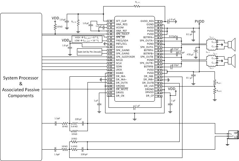 Figure 67. Stereo BTL Using Hardware Control
9.2.2.1 Design Requirements
For this design example, use the parameters listed in Table 22 as the input parameters.
Table 22. Design Parameters
| PARAMETER | EXAMPLE |
|---|---|
| Low Power Supply | 3.3 V |
| High Power Supply | 5 V to 24 V |
| Host Processor | I2S Compliant Master |
| GPIO Control | |
| Output Filters | Inductor-Capacitor Low Pass Filter |
| Speakers | 4 Ω to 8 Ω |
9.2.2.2 Detailed Design Procedure
9.2.2.2.1 Startup Procedures- Hardware Control Mode
- Configure all hardware pins as required by the application using PCB connections (that is PBTL, FREQ, GAIN, etc.)
- Start with SPK_SD pin pulled LOW and SPK_SLEEP/ADR pin pulled HIGH
- Bring up power supplies (it does not matter if PVDD/AVDD or DVDD comes up first, provided the device is held in shutdown.)
- Once power supplies are stable, start MCLK, SCLK, LRCK
- Once power supplies and clocks are stable and all hardware control pins have been configured, bring SPK_SD HIGH
- Once the device is out of shutdown mode, bring SPK_SLEEP/ADR LOW
- The device is now in normal operation
9.2.2.2.2 Shutdown Procedures- Hardware Control Mode
- The device is in normal operation
- Pull SPK_SLEEP/ADR HIGH
- Pull SPK_SD LOW
- The clocks can now be stopped and the power supplies brought down
- The device is now fully shutdown and powered off
9.2.2.2.3 Digital I/O Connectivity
The digital I/O lines of the TAS5760MD are described in previous sections. As discussed, whenever a static digital pin (that is a pin that is hardwired to be HIGH or LOW) is required to be pulled HIGH, it should be connected to DVDD through a pullup resistor in order to control the slew rate of the voltage presented to the digital I/O pins. It is not, however, necessary to have a separate pullup resistor for each static digital I/O line. Instead, a single resistor can be used to tie all static I/O lines HIGH to reduce BOM count. For instance, if Software Control Mode is desired both the GAIN[1:0] and the PBTL/SCL pins can both be pulled HIGH through a single pullup resistor.
9.2.2.3 Application Curve
Table 23. Relevant Performance Plots
| PLOT TITLE | PLOT NUMBER |
|---|---|
| Figure 1. Output Power vs PVDD | G001 |
| Figure 2. THD+N vs Frequency With PVDD = 12 V, POSPK = 1 W | G024 |
| Figure 3. THD+N vs Frequency With PVDD = 24 V, POSPK = 1 W | G025 |
| Figure 4. Idle Channel Noise vs PVDD | G026 |
| Figure 5. THD+N vs Output Power With PVDD = 12 V, Both Channels Driven | G027 |
| Figure 6. THD+N vs Output Power With PVDD = 18 V, Both Channels Driven | G028 |
| Figure 7. THD+N vs Output Power With PVDD = 24 V, Both Channels Driven | G029 |
| Figure 8. Efficiency vs Output Power | G030 |
| Figure 9. Crosstalk vs Frequency | G031 |
| Figure 10. PVDD PSRR vs Frequency | G019 |
| Figure 11. DVDD PSRR vs Frequency | G020 |
| Figure 12. Idle Current Draw vs PVDD (Filterless) | G042 |
| Figure 13. Idle Current Draw vs PVDD (With LC Filter as Shown on the EVM) | G023 |
| Figure 14. Shutdown Current Draw vs PVDD (Filterless) | G022 |
| Figure 15. Output Power vs PVDD | G039 |
| Figure 16. THD+N vs Frequency With PVDD = 12 V, POSPK = 1 W | G002 |
| Figure 17. THD+N vs Frequency With PVDD = 24 V, POSPK = 1 W | G003 |
| Figure 18. Idle Channel Noise vs PVDD | G006 |
| Figure 19. THD+N vs Output Power With PVDD = 12 V, Both Channels Driven | G008 |
| Figure 20. THD+N vs Output Power With PVDD = 18 V, Both Channels Driven | G009 |
| Figure 21. THD+N vs Output Power With PVDD = 24 V, Both Channels Driven | G010 |
| Figure 22. Efficiency vs Output Power | G014 |
| Figure 23. Crosstalk vs Frequency | G018 |
| Figure 24. PVDD PSRR vs Frequency | G019 |
| Figure 25. Idle Current Draw vs PVDD (Filterless) | G045 |
| Figure 26. Idle Current Draw vs PVDD (With LC Filter as Shown on EVM) | G044 |
| Figure 27. Shutdown Current Draw vs PVDD (Filterless) | G022 |
9.2.3 Mono PBTL Using Software Control
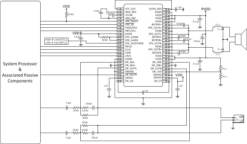 Figure 68. Mono PBTL Using Software Control
9.2.3.1 Design Requirements
For this design example, use the parameters listed in Table 24 as the input parameters.
Table 24. Design Parameters
| PARAMETER | EXAMPLE |
|---|---|
| Low Power Supply | 3.3 V |
| High Power Supply | 5 V to 24 V |
| Host Processor | I2S Compliant Master |
| I2C Compliant Master | |
| GPIO Control | |
| Output Filters | Inductor-Capacitor Low Pass Filter |
| Speakers | 4 Ω to 8 Ω |
9.2.3.2 Detailed Design Procedure
9.2.3.2.1 Startup Procedures- Software Control Mode
- Configure all digital I/O pins as required by the application using PCB connections (that is SPK_GAIN[1:0] = 11, ADR, etc.)
- Start with SPK_SD Pin = LOW
- Bring up power supplies (it does not matter if PVDD/AVDD or DVDD comes up first, provided the device is held in shutdown.)
- Once power supplies are stable, start MCLK, SCLK, LRCK
- Configure the device via the control port in the manner required by the use case, making sure to mute the device via the control port
- Once power supplies and clocks are stable and the control port has been programmed, bring SPK_SD HIGH
- Unmute the device via the control port
- The device is now in normal operation
NOTE
Control port register changes should only occur when the device is placed into shutdown. This can be accomplished either by pulling the SPK_SD pin LOW or clearing the SPK_SD bit in the control port.
9.2.3.2.2 Shutdown Procedures- Software Control Mode
- The device is in normal operation
- Mute via the control port
- Pull SPK_SD LOW
- The clocks can now be stopped and the power supplies brought down
- The device is now fully shutdown and powered off
NOTE
Any control port register changes excluding volume control changes should only occur when the device is placed into shutdown. This can be accomplished either by pulling the SPK_SD pin LOW or clearing the SPK_SD bit in the control port.
9.2.3.2.3 Component Selection and Hardware Connections
Figure 68 above details the typical connections required for proper operation of the device. It is with this list of components that the device was simulated, tested, and characterized. Deviation from this typical application circuit unless recommended by this document may produce unwanted results, which could range from degradation of audio performance to destructive failure of the device.
9.2.3.2.3.1 I²C Pull-Up Resistors
It is important to note that when the device is operated in Software Control Mode, the customary pull-up resistors are required on the SCL and SDA signal lines. They are not shown in the Typical Application Circuits, since they are shared by all of the devices on the I²C bus and are considered to be part of the associated passive components for the System Processor. These resistor values should be chosen per the guidance provided in the I²C Specification.
9.2.3.2.3.2 Digital I/O Connectivity
The digital I/O lines of the TAS5760MD are described in previous sections. As discussed, whenever a static digital pin (that is a pin that is hardwired to be HIGH or LOW) is required to be pulled HIGH, it should be connected to DVDD through a pullup resistor in order to control the slew rate of the voltage presented to the digital I/O pins. It is not, however, necessary to have a separate pullup resistor for each static digital I/O line. Instead, a single resistor can be used to tie all static I/O lines HIGH to reduce BOM count. For instance, if Software Control Mode is desired both the GAIN[1:0] and the PBTL/SCL pins can both be pulled HIGH through a single pullup resistor.
9.2.3.3 Application Curve
Table 25. Relevant Performance Plots
| PLOT TITLE | PLOT NUMBER |
|---|---|
| Figure 28. THD+N vs Frequency With PVDD = 12 V, POSPK = 1 W | G032 |
| Figure 29. THD+N vs Frequency With PVDD = 24 V, POSPK = 1 W | G033 |
| Figure 31. THD+N vs Output Power With PVDD = 12 V With 1 kHz Sine Input | G035 |
| Figure 32. THD+N vs Output Power With PVDD = 18 V With 1 kHz Sine Input | G036 |
| Figure 33. THD+N vs Output Power With PVDD = 24 V With 1 kHz Sine Input | G037 |
| Figure 34. Efficiency vs Output Power | G038 |
| Figure 35. THD+N vs Frequency With PVDD = 12 V, POSPK = 1 W | G004 |
| Figure 36. THD+N vs Frequency With PVDD = 24 V, POSPK = 1 W | G005 |
| Figure 38. THD+N vs Output Power With PVDD = 12 V | G011 |
| Figure 39. THD+N vs Output Power With PVDD = 18 V | G012 |
| Figure 40. THD+N vs Output Power With PVDD = 24 V | G013 |
| Figure 41. Efficiency vs Output Power | G015 |
9.2.4 Mono PBTL Using Hardware Control
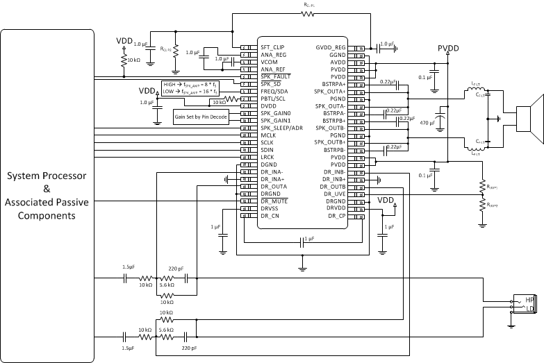 Figure 69. Mono PBTL Using Hardware Control
9.2.4.1 Design Requirements
For this design example, use the parameters listed in Table 26 as the input parameters.
Table 26. Design Parameters
| PARAMETER | EXAMPLE |
|---|---|
| Low Power Supply | 3.3 V |
| High Power Supply | 5 V to 24 V |
| Host Processor | I2S Compliant Master |
| GPIO Control | |
| Output Filters | Inductor-Capacitor Low Pass Filter |
| Speakers | 4 Ω to 8 Ω |
9.2.4.2 Detailed Design Procedure
9.2.4.2.1 Startup Procedures- Hardware Control Mode
- Configure all hardware pins as required by the application using PCB connections (that is PBTL, FREQ, GAIN, etc.)
- Start with SPK_SD pin pulled LOW and SPK_SLEEP/ADR pin pulled HIGH
- Bring up power supplies (it does not matter if PVDD/AVDD or DVDD comes up first, provided the device is held in shutdown.)
- Once power supplies are stable, start MCLK, SCLK, LRCK
- Once power supplies and clocks are stable and all hardware control pins have been configured, bring SPK_SD HIGH
- Once the device is out of shutdown mode, bring SPK_SLEEP/ADR LOW
- The device is now in normal operation
9.2.4.2.2 Shutdown Procedures- Hardware Control Mode
- The device is in normal operation
- Pull SPK_SLEEP/ADR HIGH
- Pull SPK_SD LOW
- The clocks can now be stopped and the power supplies brought down
- The device is now fully shutdown and powered off
9.2.4.2.3 Component Selection and Hardware Connections
Figure 69 details the typical connections required for proper operation of the device. It is with this list of components that the device was simulated, tested, and characterized. Deviation from this typical application circuit unless recommended by this document may produce unwanted results, which could range from degradation of audio performance to destructive failure of the device.
9.2.4.2.4 Digital I/O Connectivity
The digital I/O lines of the TAS5760MD are described in previous sections. As discussed, whenever a static digital pin (that is a pin that is hardwired to be HIGH or LOW) is required to be pulled HIGH, it should be connected to DVDD through a pullup resistor in order to control the slew rate of the voltage presented to the digital I/O pins. It is not, however, necessary to have a separate pullup resistor for each static digital I/O line. Instead, a single resistor can be used to tie all static I/O lines HIGH to reduce BOM count. For instance, if Software Control Mode is desired both the GAIN[1:0] and the PBTL/SCL pins can both be pulled HIGH through a single pullup resistor.
9.2.4.3 Application Curve
Table 27. Relevant Performance Plots
| PLOT TITLE | PLOT NUMBER |
|---|---|
| Figure 28. THD+N vs Frequency With PVDD = 12 V, POSPK = 1 W | G032 |
| Figure 29. THD+N vs Frequency With PVDD = 24 V, POSPK = 1 W | G033 |
| Figure 30. Idle Channel Noise vs PVDD | G034 |
| Figure 31. THD+N vs Output Power With PVDD = 12 V With 1 kHz Sine Input | G035 |
| Figure 32. THD+N vs Output Power With PVDD = 18 V With 1 kHz Sine Input | G036 |
| Figure 33. THD+N vs Output Power With PVDD = 24 V With 1 kHz Sine Input | G037 |
| Figure 34. Efficiency vs Output Power | G038 |
| Figure 35. THD+N vs Frequency With PVDD = 12 V, POSPK = 1 W | G004 |
| Figure 36. THD+N vs Frequency With PVDD = 24 V, POSPK = 1 W | G005 |
| Figure 37. Idle Channel Noise vs PVDD | G007 |
| Figure 38. THD+N vs Output Power With PVDD = 12 V | G011 |
| Figure 39. THD+N vs Output Power With PVDD = 18 V | G012 |
| Figure 40. THD+N vs Output Power With PVDD = 24 V | G013 |
| Figure 41. Efficiency vs Output Power | G015 |
