SLOS841B September 2013 – January 2015 TPA3131D2 , TPA3132D2
PRODUCTION DATA.
- 1 Features
- 2 Applications
- 3 Description
- 4 Revision History
- 5 Pin Configuration and Functions
- 6 Specifications
-
7 Detailed Description
- 7.1 Overview
- 7.2 Functional Block Diagram
- 7.3
Feature Description
- 7.3.1 Gain Setting and Master and Slave
- 7.3.2 Input Impedance
- 7.3.3 Start-up/Shutdown Operation
- 7.3.4 PLIMIT Operation
- 7.3.5 GVDD Supply
- 7.3.6 BSPx and BSNx Capacitors
- 7.3.7 Differential Inputs
- 7.3.8 Device Protection System
- 7.3.9 DC Detect Protection
- 7.3.10 Short-Circuit Protection and Automatic Recovery Feature
- 7.3.11 Thermal Protection
- 7.3.12 Efficiency: LC Filter Required with the Traditional Class-D Modulation Scheme
- 7.3.13 Ferrite Bead Filter Considerations
- 7.3.14 When to Use an Output Filter for EMI Suppression
- 7.3.15 AM Avoidance EMI Reduction
- 7.4 Device Functional Modes
- 8 Applications and Implementation
- 9 Power Supply Recommendations
- 10Layout
- 11Device and Documentation Support
- 12Mechanical, Packaging, and Orderable Information
7 Detailed Description
7.1 Overview
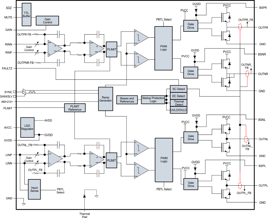
The TPA3132D2 device is a high-efficiency stereo Class-D audio power amplifier optimized for high-transient power capability to utilize the dynamic power headroom of small loudspeakers. It’s capable of delivering high peak power into a 4-Ω speaker.
The device can be configured for either master or slave operation by using the SYNC pin. This helps to prevent audible beats noise.
7.2 Functional Block Diagram
7.3 Feature Description
7.3.1 Gain Setting and Master and Slave
The gain of the TPA3131D2 is set by the voltage divider connected to the GAIN/SLV control pin. Master or Slave mode is also controlled by the same pin. An internal ADC is used to detect the 8 input states. The first four stages sets the GAIN in Master mode in gains of 20, 26, 32, 36 dB respectively, while the next four stages sets the GAIN in Slave mode in gains of 20, 26, 32, 36 dB respectively. The gain setting is latched during power-up and cannot be changed while device is powered. shows the recommended resistor values and the state and gain:
Table 1. Gain and Master/Slave
| MASTER / SLAVE MODE | GAIN | R1 (to GND) | R2 (to GVDD) | INPUT IMPEDANCE |
|---|---|---|---|---|
| Master | 20 dB | 5.6 kΩ | OPEN | 60 kΩ |
| Master | 26 dB | 20 kΩ | 100 kΩ | 30 kΩ |
| Master | 32 dB | 39 kΩ | 100 kΩ | 15 kΩ |
| Master | 36 dB | 47 kΩ | 75 kΩ | 9 kΩ |
| Slave | 20 dB | 51 kΩ | 51 kΩ | 60 kΩ |
| Slave | 26 dB | 75 kΩ | 47 kΩ | 30 kΩ |
| Slave | 32 dB | 100 kΩ | 39 kΩ | 15 kΩ |
| Slave | 36 dB | 100 kΩ | 16 kΩ | 9 kΩ |
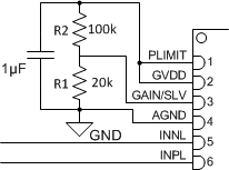 Figure 19. Gain and Master/Slave Select Resistors
In Master mode, SYNC terminal is an output, in Slave mode, SYNC terminal is an input for a clock input. TTL logic levels with compliance to GVDD.
7.3.2 Input Impedance
The TPA313xD2 input stage is a fully differential input stage and the input impedance changes with the gain setting from 9 kΩ at 36 dB gain to 60 kΩ at 20 dB gain. Table 1 lists the values from min to max gain. The tolerance of the input resistor value is ±20% so the minimum value will be higher than 7.2 kΩ. The inputs need to be AC-coupled to minimize the output dc-offset and ensure correct ramping of the output voltages during power-ON and power-OFF. The input ac-coupling capacitor together with the input impedance forms a high-pass filter with the following cut-off frequency:

If a flat bass response is required down to 20 Hz the recommended cut-off frequency is a tenth of that, 2 Hz. lists the recommended ac-couplings capacitors for each gain step. If a -3 dB is accepted at 20 Hz 10 times lower capacitors can used – for example, a 1 µF can be used.
Table 2. Recommended Input AC-Coupling Capacitors
| GAIN | INPUT IMPEDANCE | INPUT CAPACITANCE | HIGH-PASS FILTER |
|---|---|---|---|
| 20 dB | 60 kΩ | 1.5 µF | 1.8 Hz |
| 26 dB | 30 kΩ | 3.3 µF | 1.6 Hz |
| 32 dB | 15 kΩ | 5.6 µF | 2.3 Hz |
| 36 dB | 9 kΩ | 10 µF | 1.8 Hz |
 Figure 20. Input AC Coupling
The input capacitors used should be a type with low leakage, like quality electrolytic, tantalum or ceramic. If a polarized type is used the positive connection should face the input pins which are biased to 3 Vdc.
7.3.3 Start-up/Shutdown Operation
The TPA313xD2 employs a shutdown mode of operation designed to reduce supply current (Icc) to the absolute minimum level during periods of nonuse for power conservation. The SDZ input terminal should be held high (see specification table for trip point) during normal operation when the amplifier is in use. Pulling SDZ low will put the outputs to mute and the amplifier to enter a low-current state. It is not recommended to leave SDZ unconnected, because amplifier operation would be unpredictable.
For the best power-off pop performance, place the amplifier in the shutdown mode prior to removing the power supply. The gain setting is selected at the end of the start-up cycle. At the end of the start-up cycle, the gain is selected and cannot be changed until the next power-up.
7.3.4 PLIMIT Operation
The TPA313xD2 has a built-in voltage limiter that can be used to limit the output voltage level below the supply rail, the amplifier simply operates as if it was powered by a lower supply voltage, and thereby limits the output power. Add a resistor divider from GVDD to ground to set the voltage at the PLIMIT pin. An external reference may also be used if tighter tolerance is required. Add a 1 µF capacitor from pin PLIMIT to ground to ensure stability.
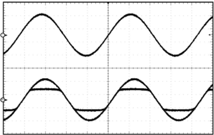 Figure 21. Power Limit Example
The PLIMIT circuit sets a limit on the output peak-to-peak voltage. The limiting is done by limiting the duty cycle to a fixed maximum value. This limit can be thought of as a "virtual" voltage rail which is lower than the supply connected to PVCC. This "virtual" rail is approximately 4 times the voltage at the PLIMIT pin. This output voltage can be used to calculate the maximum output power for a given maximum input voltage and speaker impedance.

where
- POUT (10%THD) = 1.25 × POUT (unclipped)
- RL is the load resistance.
- RS is the total series resistance including RDS(on), and output filter resistance.
- VP is the peak amplitude
- VP = 4 × PLIMIT voltage if PLIMIT < 4 × VP
Increasing the PLIMIT voltage from a given value increases the maximum output voltage swing until it equals PVCC. Adjusting PLIMIT to a higher value will disable the PLIMIT function and will offer highest available output power, however for TPA3131D2 and TPA3132D2 it is always advised to use the PLIMIT function if PVCC is higher than nominal value to prevent shutdown due to over current protection. If PLIMIT is disabled on TPA3131D2 and TPA3132D2 an over current shutdown can occur with minimum recommended load impedance when PVCC is higher than its nominal value. To disable the PLIMIT function, the PLIMIT pin is simply connected to GVDD.
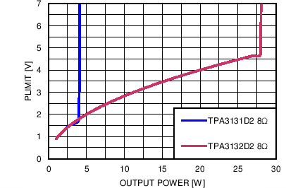 Figure 22. PLIMIT vs. Max. Output Power, 8Ω load
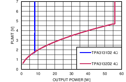 Figure 23. PLIMIT vs. Max. Output Power, 4Ω load
Table 3. Power Limit Example
| MINIMUM PVCC (V) | PART NUMBERS | PLIMIT VOLTAGE (V)(1) | R to GND | R to GVDD | OUTPUT POWER 8Ω (W) |
|---|---|---|---|---|---|
| 7.4 V | TPA3131D2, TPA3132D2 | 1.85 | 27 kΩ | 75 kΩ | 4 |
| 12 V | TPA3132D2 | 2.87 | 39 kΩ | 56 kΩ | 10 |
| 19 V | TPA3132D2 | 4.26 | 56 kΩ | 36 kΩ | 25 |
7.3.5 GVDD Supply
The GVDD Supply is used to power the gates of the output full bridge transistors. It can also be used to supply the PLIMIT and GAIN/SLV voltage dividers. Decouple GVDD with a X5R ceramic 1 µF capacitor to GND. The GVDD supply is not intended to be used for external supply. It is recommended to limit the current consumption by using resistor voltage dividers for GAIN/SLV and PLIMIT of 100 kΩ or more.
7.3.6 BSPx and BSNx Capacitors
The full H-bridge output stages use only NMOS transistors. Therefore, they require bootstrap capacitors for the high side of each output to turn on correctly. A 220 nF ceramic capacitor of quality X5R or better, rated for at least 16 V, must be connected from each output to its corresponding bootstrap input. (See the application circuit diagram in Figure 29.) The bootstrap capacitors connected between the BSxx pins and corresponding output function as a floating power supply for the high-side N-channel power MOSFET gate drive circuitry. During each high-side switching cycle, the bootstrap capacitors hold the gate-to-source voltage high enough to keep the high-side MOSFETs turned on.
7.3.7 Differential Inputs
The differential input stage of the amplifier cancels any noise that appears on both input lines of the channel. To use the TPA313xD2 with a differential source, connect the positive lead of the audio source to the RINP or LINP input and the negative lead from the audio source to the RINN or LINN input. To use the TPA313xD2 with a single-ended source, ac ground the negative input through a capacitor equal in value to the input capacitor on positive and apply the audio source to either input. In a single-ended input application, the unused input should be ac grounded at the audio source instead of at the device input for best noise performance. For good transient performance, the impedance seen at each of the two differential inputs should be the same.
The impedance seen at the inputs should be limited to an RC time constant of 1 ms or less if possible. This is to allow the input dc blocking capacitors to become completely charged during the 10 ms power-up time. If the input capacitors are not allowed to completely charge, there will be some additional sensitivity to component matching which can result in pop if the input components are not well matched.
7.3.8 Device Protection System
The TPA313xD2 contains a complete set of protection circuits carefully designed to make system design efficient as well as to protect the device against any kind of permanent failures due to short circuits, overload, over temperature, and under-voltage. The FAULTZ pin will signal if an error is detected according to the fault table below:
Table 4. Fault Reporting
| FAULT | TRIGGERING CONDITION (typical value) |
FAULTZ | ACTION | LATCHED/SELF-CLEARING |
|---|---|---|---|---|
| Over Current | Output short or short to PVCC or GND | Low | Output high impedance | Latched |
| Over Temperature | Tj > 150°C | Low | Output high impedance | Latched |
| Too High DC Offset | DC output voltage | Low | Output high impedance | Latched |
| Under Voltage on PVCC | PVCC < 4.5V | – | Output high impedance | Self-clearing |
| Over Voltage on PVCC | PVCC > 27V | – | Output high impedance | Self-clearing |
7.3.9 DC Detect Protection
The TPA313xD2 has circuitry which will protect the speakers from DC current which might occur due to defective capacitors on the input or shorts on the printed circuit board at the inputs. A DC detect fault will be reported on the FAULT pin as a low state. The DC Detect fault will also cause the amplifier to shutdown by changing the state of the outputs to Hi-Z.
If automatic recovery from the short circuit protection latch is desired, connect the FAULTZ pin directly to the SDZ pin. This allows the DC Protection function to automatically drive the SDZ pin low which clears the DC Detect protection latch.
A DC Detect Fault is issued when the output differential duty-cycle of either channel exceeds 60% for more than 420 msec at the same polarity. Table x below shows some examples of the typical DC Detect Protection threshold for several values of the supply voltage. This feature protects the speaker from large DC currents or AC currents less than 2Hz. To avoid nuisance faults due to the DC detect circuit, hold the SD pin low at power-up until the signals at the inputs are stable. Also, take care to match the impedance seen at the positive and negative inputs to avoid nuisance DC detect faults.
The minimum output offset voltages required to trigger the DC detect are show in Table 5. The outputs must remain at or above the voltage listed in the table for more than 420 msec to trigger the DC detect.
Table 5. DC Detect Threshold
| PVCC (V) | VOS - OUTPUT OFFSET VOLTAGE (V) |
|---|---|
| 4.5 | 0.96 |
| 6 | 1.3 |
| 12 | 2.6 |
| 18 | 3.9 |
7.3.10 Short-Circuit Protection and Automatic Recovery Feature
The TPA313xD2 has protection from over current conditions caused by a short circuit on the output stage. The short circuit protection fault is reported on the FAULTZ pin as a low state. The amplifier outputs are switched to a high impedance state when the short circuit protection latch is engaged. The latch can be cleared by cycling the SDZ pin through the low state.
If automatic recovery from the short circuit protection latch is desired, connect the FAULTZ pin directly to the SDZ pin. This allows the FAULTZ pin function to automatically drive the SDZ pin low which clears the short-circuit protection latch.
In systems where a possibility of a permanent short from the output to PVDD or to a high voltage battery like a car battery can occur, pull the MUTE pin low with the FAULTZ signal with a inverting transistor to ensure a high-Z restart, like shown in the figure below:
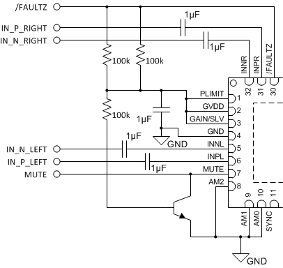 Figure 24. MUTE Driven by Inverted FAULTZ
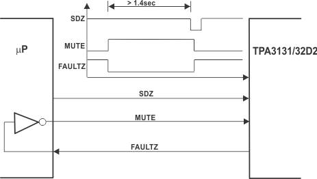 Figure 25. Timing Requirement for SDZ
7.3.11 Thermal Protection
Thermal protection on the TPA313xD2 prevents damage to the device when the internal die temperature exceeds 150°C. There is a ±15°C tolerance on this trip point from device to device. Once the die temperature exceeds the thermal trip point, the device enters into the shutdown state and the outputs are disabled. This is a latched fault.
Thermal protection faults are reported on the FAULTZ terminal as a low state.
If automatic recovery from the thermal protection latch is desired, connect the FAULTZ pin directly to the SDZ pin. This allows the FAULTZ pin function to automatically drive the SDZ pin low which clears the thermal protection latch.
7.3.12 Efficiency: LC Filter Required with the Traditional Class-D Modulation Scheme
The main reason that the traditional class-D amplifier-based on AD modulation needs an output filter is that the switching waveform results in maximum current flow. This causes more loss in the load, which causes lower efficiency. The ripple current is large for the traditional modulation scheme, because the ripple current is proportional to voltage multiplied by the time at that voltage. The differential voltage swing is 2 × VCC, and the time at each voltage is half the period for the traditional modulation scheme. An ideal LC filter is needed to store the ripple current from each half cycle for the next half cycle, while any resistance causes power dissipation. The speaker is both resistive and reactive, whereas an LC filter is almost purely reactive.
The TPA313xD2 modulation scheme has little loss in the load without a filter because the pulses are short and the change in voltage is VCC instead of 2 × VCC. As the output power increases, the pulses widen, making the ripple current larger. Ripple current could be filtered with an LC filter for increased efficiency, but for most applications the filter is not needed.
An LC filter with a cutoff frequency less than the class-D switching frequency allows the switching current to flow through the filter instead of the load. The filter has less resistance but higher impedance at the switching frequency than the speaker, which results in less power dissipation, therefore increasing efficiency.
7.3.13 Ferrite Bead Filter Considerations
Using the Advanced Emissions Suppression Technology in the TPA313xD2 amplifier it is possible to design a high efficiency class-D audio amplifier while minimizing interference to surrounding circuits. It is also possible to accomplish this with only a low-cost ferrite bead filter. In this case it is necessary to carefully select the ferrite bead used in the filter. One important aspect of the ferrite bead selection is the type of material used in the ferrite bead. Not all ferrite material is alike, so it is important to select a material that is effective in the 10 to 100 MHz range which is key to the operation of the class-D amplifier. Many of the specifications regulating consumer electronics have emissions limits as low as 30 MHz. It is important to use the ferrite bead filter to block radiation in the 30 MHz and above range from appearing on the speaker wires and the power supply lines which are good antennas for these signals. The impedance of the ferrite bead can be used along with a small capacitor with a value in the range of 1000 pF to reduce the frequency spectrum of the signal to an acceptable level. For best performance, the resonant frequency of the ferrite bead/ capacitor filter should be less than 10 MHz.
Also, it is important that the ferrite bead is large enough to maintain its impedance at the peak currents expected for the amplifier. Some ferrite bead manufacturers specify the bead impedance at a variety of current levels. In this case it is possible to make sure the ferrite bead maintains an adequate amount of impedance at the peak current the amplifier will see. If these specifications are not available, it is also possible to estimate the bead current handling capability by measuring the resonant frequency of the filter output at low power and at maximum power. A change of resonant frequency of less than fifty percent under this condition is desirable. Examples of ferrite beads which have been tested and work well with the TPA3130D2 can be seen in the TPA3130D2EVM user guide SLOU341.
A high quality ceramic capacitor is also needed for the ferrite bead filter. A low ESR capacitor with good temperature and voltage characteristics will work best.
Additional EMC improvements may be obtained by adding snubber networks from each of the class-D outputs to ground. Suggested values for a simple RC series snubber network would be 18 Ω in series with a 330 pF capacitor although design of the snubber network is specific to every application and must be designed taking into account the parasitic reactance of the printed circuit board as well as the audio amp. Take care to evaluate the stress on the component in the snubber network especially if the amp is running at high PVCC. Also, make sure the layout of the snubber network is tight and returns directly to the GND pins on the IC.
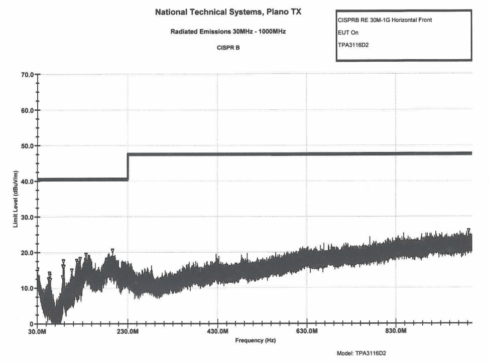 Figure 26. TPA311xD2 Radiated Emissions
7.3.14 When to Use an Output Filter for EMI Suppression
The TPA313xD2 has been tested with a simple ferrite bead filter for a variety of applications including long speaker wires up to 125 cm and high power. The TPA313xD2 EVM passes FCC class-B specifications under these conditions using twisted speaker wires. The size and type of ferrite bead can be selected to meet application requirements. Also, the filter capacitor can be increased if necessary with some impact on efficiency.
There may be a few circuit instances where it is necessary to add a complete LC reconstruction filter. These circumstances might occur if there are nearby circuits which are sensitive to noise. In these cases a classic second order Butterworth filter similar to those shown in the figures below can be used.
Some systems have little power supply decoupling from the AC line but are also subject to line conducted interference (LCI) regulations. These include systems powered by "wall warts" and "power bricks." In these cases, LC reconstruction filters can be the lowest cost means to pass LCI tests. Common mode chokes using low frequency ferrite material can also be effective at preventing line conducted interference.
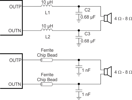 Figure 27. Output Filter Configurations
7.3.15 AM Avoidance EMI Reduction
To reduce interference in the AM radio band, the TPA313xD2 has the ability to change the switching frequency via AM<2:0> pins. The recommended frequencies are listed in Table 6. The fundamental frequency and its second harmonic straddle the AM radio band listed. This eliminates the tones that can be present due to the switching frequency being demodulated by the AM radio.
Table 6. AM Frequencies
| US | EUROPEAN | ||||
|---|---|---|---|---|---|
| AM FREQUENCY (kHz) | AM FREQUENCY (kHz) | SWITCHING FREQUENCY (kHz) | AM2 | AM1 | AM0 |
| 522-540 | |||||
| 540-917 | 540-914 | 500 | 0 | 0 | 1 |
| 917-1125 | 914-1122 | 600 (or 400) | 0 | 1 | 0 |
| 0 | 0 | 0 | |||
| 1125-1375 | 1122-1373 | 500 | 0 | 0 | 1 |
| 1375-1547 | 1373-1548 | 600 (or 400) | 0 | 1 | 0 |
| 0 | 0 | 0 | |||
| 1547-1700 | 1548-1701 | 600 (or 500) | 0 | 1 | 0 |
| 0 | 0 | 1 | |||
7.4 Device Functional Modes
7.4.1 Mono Mode (PBTL)
The TPA313xD2 can be connected in MONO mode enabling up to 85W output power. This is done by:
- Connect INPL and INNL directly to Ground (without capacitors) this sets the device in Mono mode during power up.
- Connect OUTPR and OUTNR together for the positive speaker terminal and OUTNL and OUTPL together for the negative terminal.
- Analog input signal is applied to INPR and INNR.
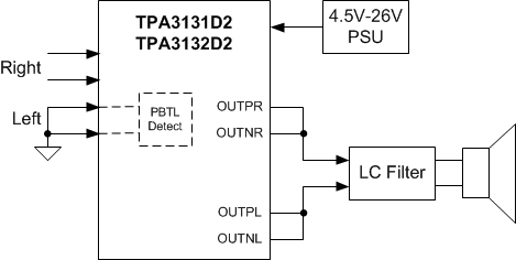 Figure 28. Output Mode select