SLOU560 July 2022 TAS2781
8 Schematic and Layout Guidelines
This section provides a list of important items to consider during component selection as well as layout. Following these guidelines help for proper device performance and operation.
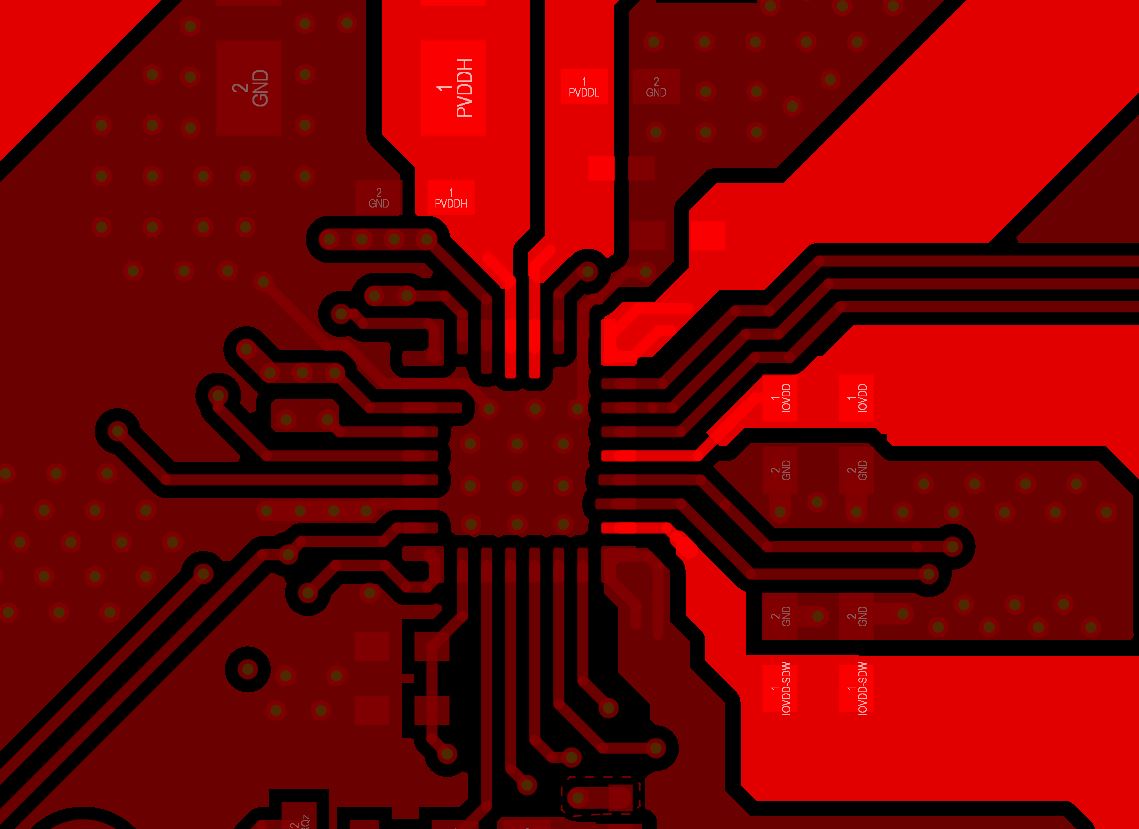
- All supply rails should be bypassed by low-ESR ceramic capacitors. Consider capacitance derating due to DC as this is considerably critical for higher power rails, a good rule of thumb is to select capacitors with rated voltage 2 or 3 times the supply rail voltage.
 Figure 8-1 Supply Rails Layout
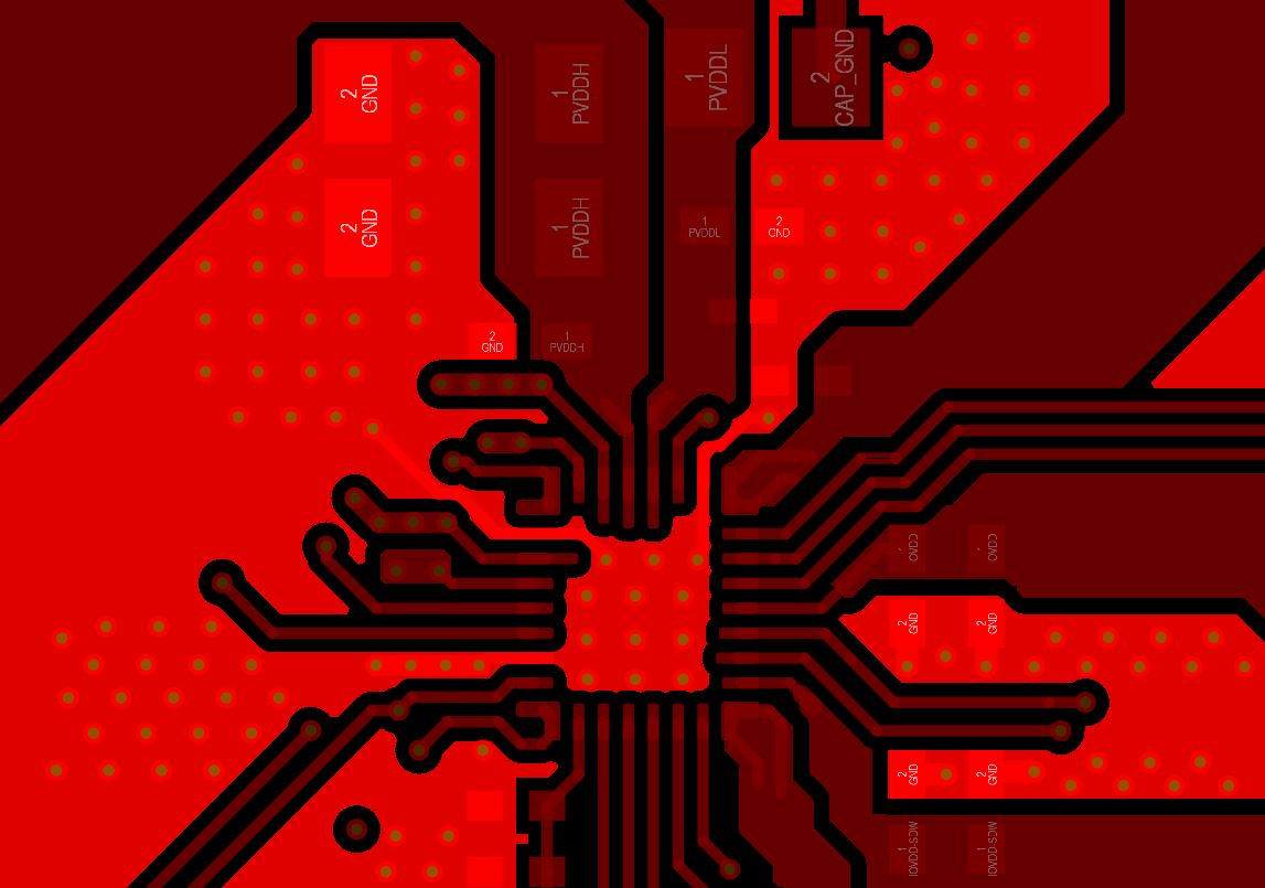
 - Use GND planes with multiple conductive epoxy filled vias to create a low impedance connection to PGND and GND, this also helps to minimize the GND noise. The layout design must target minimum parasitic loop inductance between PVDDH, PGND pins and decoupling capacitor.
 Figure 8-2 GND Layout
 - Use wider traces that carry high current such as PVDDH, PVDDL, OUT_P and OUT_N.
- Connect VSNS_P and VSNS_N as close as possible to the speaker.
- VSNS_P and VSNS_N should be connected between the EMI ferrite filter and the speaker if EMI ferrites are used at the outputs.
- VSNS_P and VSNS_N routing should be separated and shielded from switching signals such as interface signals, speaker outputs and bootstrap pins.
- Place bootstrap capacitors as close as possible to the BSTP/N pins.
 Figure 8-3 Bootstrap and Outputs Layout