DATA SHEET
CSD18537NQ5A 60-V N-Channel NexFET Power MOSFETs
1 Features
2 Applications
- High-Side Synchronous Buck Converter
- Motor Control
3 Description
This 10 mΩ, 60 V, SON 5 mm x 6 mm NexFET™power MOSFET is designed to minimize losses in power conversion applications.
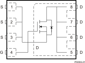
Top View
Product Summary
| TA = 25°C | TYPICAL VALUE | UNIT | ||
|---|---|---|---|---|
| VDS | Drain-to-Source Voltage | 60 | V | |
| Qg | Gate Charge Total (10 V) | 14 | nC | |
| Qgd | Gate Charge Gate-to-Drain | 2.3 | nC | |
| RDS(on) | Drain-to-Source On Resistance | VGS = 6 V | 13 | mΩ |
| VGS = 10 V | 10 | mΩ | ||
| VGS(th) | Threshold Voltage | 3 | V | |
Ordering Information(1)
| Device | Qty | Media | Package | Ship |
|---|---|---|---|---|
| CSD18537NQ5A | 2500 | 13-Inch Reel | SON 5 x 6 mm Plastic Package | Tape and Reel |
| CSD18537NQ5AT | 250 | 7-Inch Reel |
- For all available packages, see the orderable addendum at the end of the data sheet.
Absolute Maximum Ratings
| TA = 25°C | VALUE | UNIT | |
|---|---|---|---|
| VDS | Drain-to-Source Voltage | 60 | V |
| VGS | Gate-to-Source Voltage | ±20 | V |
| ID | Continuous Drain Current (Package limited) | 50 | A |
| Continuous Drain Current (Silicon limited), TC = 25°C | 54 | ||
| Continuous Drain Current(1) | 11 | ||
| IDM | Pulsed Drain Current(2) | 151 | A |
| PD | Power Dissipation(1) | 3.2 | W |
| Power Dissipation, TC = 25°C | 75 | ||
| TJ, Tstg |
Operating Junction and Storage Temperature Range |
–55 to 150 | °C |
| EAS | Avalanche Energy, single pulse ID = 33 A, L = 0.1 mH, RG = 25 Ω |
55 | mJ |
RDS(on) vs VGS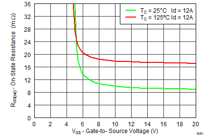 |
Gate Charge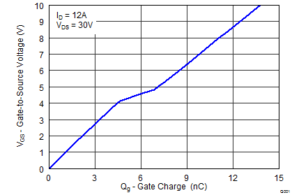 |
4 Revision History
Changes from A Revision (February 2014) to B Revision
- Reduced silicon current limit to 54 A due to increase in RθJCGo
- Increased pulsed current limit to 151 Go
- Added line for maximum power dissipation with case temperature held to 25ºC Go
- Updated the pulsed current conditions Go
- Increased the maximum RθJC to 2.1 ºC/W Go
- Updated Figure 1 from a normalized RθJA curve to an RθJC curveGo
- Updated Figure 10 to show an improved SOAGo
- Updated Figure 12 to show a 50-A package current limit Go
Changes from * Revision (June 2013) to A Revision
5 Specifications
5.1 Electrical Characteristics
(TA = 25°C unless otherwise stated)| PARAMETER | TEST CONDITIONS | MIN | TYP | MAX | UNIT | ||
|---|---|---|---|---|---|---|---|
| STATIC CHARACTERISTICS | |||||||
| BVDSS | Drain-to-Source Voltage | VGS = 0 V, ID = 250 μA | 60 | V | |||
| IDSS | Drain-to-Source Leakage Current | VGS = 0 V, VDS = 48 V | 1 | μA | |||
| IGSS | Gate-to-Source Leakage Current | VDS = 0 V, VGS = 20 V | 100 | nA | |||
| VGS(th) | Gate-to-Source Threshold Voltage | VDS = VGS, ID = 250 μA | 2.6 | 3 | 3.5 | V | |
| RDS(on) | Drain-to-Source On Resistance | VGS = 6 V, ID = 12 A | 13 | 17 | mΩ | ||
| VGS = 10 V, ID = 12 A | 10 | 13 | mΩ | ||||
| gƒs | Transconductance | VDS = 30 V, ID = 12 A | 62 | S | |||
| DYNAMIC CHARACTERISTICS | |||||||
| Ciss | Input Capacitance | VGS = 0 V, VDS = 30 V, ƒ = 1 MHz | 1140 | 1480 | pF | ||
| Coss | Output Capacitance | 136 | 177 | pF | |||
| Crss | Reverse Transfer Capacitance | 4 | 5.2 | pF | |||
| RG | Series Gate Resistance | 5.5 | 11 | Ω | |||
| Qg | Gate Charge Total (10 V) | VDS = 30 V, ID = 12 A | 14 | 18 | nC | ||
| Qgd | Gate Charge Gate-to-Drain | 2.3 | nC | ||||
| Qgs | Gate Charge Gate-to-Source | 4.7 | nC | ||||
| Qg(th) | Gate Charge at Vth | 3.3 | nC | ||||
| Qoss | Output Charge | VDS = 30 V, VGS = 0 V | 25 | nC | |||
| td(on) | Turn On Delay Time | VDS = 30 V, VGS = 10 V, IDS = 12 A, RG = 0 Ω | 5.8 | ns | |||
| tr | Rise Time | 4 | ns | ||||
| td(off) | Turn Off Delay Time | 14.4 | ns | ||||
| tƒ | Fall Time | 3.2 | ns | ||||
| DIODE CHARACTERISTICS | |||||||
| VSD | Diode Forward Voltage | ISD = 12 A, VGS = 0 V | 0.8 | 1 | V | ||
| Qrr | Reverse Recovery Charge | VDS= 30 V, IF = 12 A, di/dt = 300 A/μs | 54 | nC | |||
| trr | Reverse Recovery Time | 40 | ns | ||||
5.2 Thermal Information
(TA = 25°C unless otherwise stated)| THERMAL METRIC | MIN | TYP | MAX | UNIT | |
|---|---|---|---|---|---|
| RθJC | Junction-to-Case Thermal Resistance (1) | 2.1 | °C/W | ||
| RθJA | Junction-to-Ambient Thermal Resistance (1)(2) | 50 | |||
(1) RθJC is determined with the device mounted on a 1-inch2 (6.45-cm2), 2-oz. (0.071-mm thick) Cu pad on a 1.5-inches × 1.5-inches
(3.81-cm × 3.81-cm), 0.06-inch (1.52-mm) thick FR4 PCB. RθJC is specified by design, whereas RθJA is determined by the user’s board design.
(3.81-cm × 3.81-cm), 0.06-inch (1.52-mm) thick FR4 PCB. RθJC is specified by design, whereas RθJA is determined by the user’s board design.
(2) Device mounted on FR4 material with 1-inch2 (6.45-cm2), 2-oz. (0.071-mm thick) Cu.
 |
Max RθJA = 50°C/W when mounted on 1 inch2 (6.45 cm2) of 2-oz. (0.071-mm thick) Cu. |
 |
Max RθJA = 125°C/W when mounted on a minimum pad area of 2-oz. (0.071-mm thick) Cu. |
5.3 Typical MOSFET Characteristics
(TA = 25°C unless otherwise stated)


6 Device and Documentation Support
6.1 Trademarks
NexFET is a trademark of Texas Instruments.
6.2 Electrostatic Discharge Caution

These devices have limited built-in ESD protection. The leads should be shorted together or the device placed in conductive foam during storage or handling to prevent electrostatic damage to the MOS gates.
6.3 Glossary
SLYZ022 — TI Glossary.
This glossary lists and explains terms, acronyms, and definitions.