SLPS485C January 2014 – May 2024 CSD19536KCS
PRODUCTION DATA
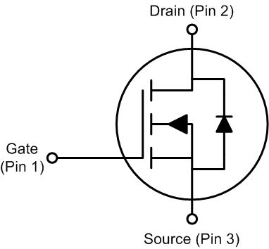
3 Description
This 100V, 2.3mΩ, TO-220 NexFET™ power MOSFET is designed to minimize losses in power conversion applications.
 |
 |
Product Summary
| TA = 25°C | TYPICAL VALUE | UNIT | ||
|---|---|---|---|---|
| VDS | Drain-to-Source Voltage | 100 | V | |
| Qg | Gate Charge Total (10V) | 118 | nC | |
| Qgd | Gate Charge Gate to Drain | 17 | nC | |
| RDS(on) | Drain-to-Source On-Resistance | VGS = 6V | 2.5 | mΩ |
| VGS = 10V | 2.3 | mΩ | ||
| VGS(th) | Threshold Voltage | 2.5 | V | |
Ordering Information
| Device | Package | Media | Qty | Ship |
|---|---|---|---|---|
| CSD19536KCS | TO-220 Plastic Package | Tube | 50 | Tube |
Absolute Maximum Ratings
| TA = 25°C | VALUE | UNIT | |
|---|---|---|---|
| VDS | Drain-to-Source Voltage | 100 | V |
| VGS | Gate-to-Source Voltage | ±20 | V |
| ID | Continuous Drain Current (Package limited) | 150 | A |
| Continuous Drain Current (Silicon limited), TC = 25°C | 259 | ||
| Continuous Drain Current (Silicon limited), TC = 100°C | 183 | ||
| IDM | Pulsed Drain Current (1) | 400 | A |
| PD | Power Dissipation | 375 | W |
| TJ, Tstg |
Operating Junction and Storage Temperature Range |
–55 to 175 | °C |
| EAS | Avalanche Energy, single pulse ID = 127A, L = 0.1mH, RG = 25Ω |
806 | mJ |
(1) Max RθJC = 0.4°C/W, pulse duration ≤100μs, duty cycle
≤1%
 vs VGS") RDS(on) vs VGS
RDS(on) vs VGS |
 Gate
Charge
Gate
Charge |