SLPS521A December   2014  – May 2024 CSD85301Q2

PRODUCTION DATA  
  1.   1
  2. 1Features
  3. 2Applications
  4. 3Description
  5. 4Specifications
    1. 4.1 Electrical Characteristics
    2. 4.2 Thermal Information
    3. 4.3 Typical MOSFET Characteristics
  6. 5Device and Documentation Support
    1. 5.1 Receiving Notification of Documentation Updates
    2. 5.2 Support Resources
    3. 5.3 Trademarks
    4. 5.4 Electrostatic Discharge Caution
    5. 5.5 Glossary
  7. 6Revision History
  8. 7Mechanical, Packaging, and Orderable Information
    1. 7.1 Package Dimensions
    2. 7.2 PCB Land Pattern
    3. 7.3 Recommended Stencil Opening
    4. 7.4 Q2 Tape and Reel Information

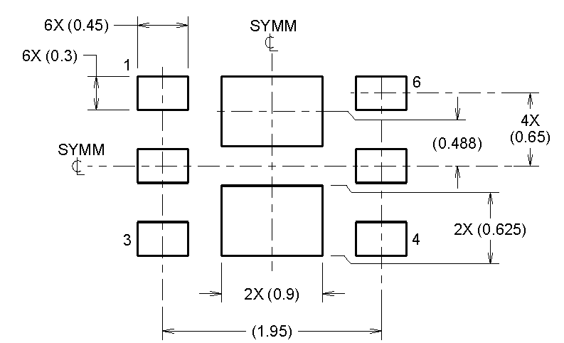
PCB Land Pattern

CSD85301Q2

For recommended circuit layout for PCB designs, see application note SLPA005Reducing Ringing Through PCB Layout Techniques.