SLPS521A December 2014 – May 2024 CSD85301Q2
PRODUCTION DATA
3 Description
The CSD85301Q2 is a 20V, 23mΩ N-Channel device with dual independent MOSFETs in a SON 2mm x 2mm plastic package. The two FETs were designed to be used in a half bridge configuration for synchronous buck and other power supply applications. Additionally, this part can be used for adaptor, USB input protection and battery charging applications. The dual FETs feature low drain to source on-resistance that minimizes losses and offers low component count for space constrained applications.
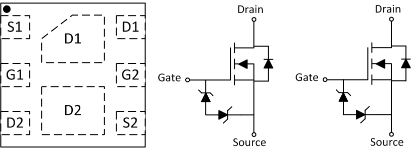
 Top View and Circuit Image
Product Summary
| TA = 25°C | TYPICAL VALUE | UNIT | ||
|---|---|---|---|---|
| VDS | Drain-to-Source Voltage | 20 | V | |
| Qg | Gate Charge Total (4.5V) | 4.2 | nC | |
| Qgd | Gate Charge Gate to Drain | 1.0 | nC | |
| RDS(on) | Drain-to-Source On Resistance | VGS = 1.8V | 65 | mΩ |
| VGS = 2.5V | 33 | mΩ | ||
| VGS = 3.8V | 25 | mΩ | ||
| VGS = 4.5V | 23 | mΩ | ||
| VGS(th) | Threshold Voltage | 0.9 | V | |
Ordering Information
| Device(1) | Media | Qty | Package | Ship |
|---|---|---|---|---|
| CSD85301Q2 | 7-Inch Reel | 3000 | SON 2mm x 2mm Plastic Package |
Tape and Reel |
| CSD85301Q2T | 7-Inch Reel | 250 |
(1) For all available packages, see the orderable addendum at the
end of the data sheet.
Absolute Maximum Ratings
| TA = 25°C | VALUE | UNIT | |
|---|---|---|---|
| VDS | Drain-to-Source Voltage | 20 | V |
| VGS | Gate-to-Source Voltage | ±10 | V |
| ID | Continuous Drain Current (Package limited) | 5.0 | A |
| IDM | Pulsed Drain Current(1) | 26 | A |
| PD | Power Dissipation(2) | 2.3 | W |
| TJ, Tstg |
Operating Junction and Storage Temperature Range |
–55 to 150 | °C |
| EAS | Avalanche Energy, single pulse ID = 8.7A, L = 0.1mH, RG = 25Ω |
3.8 | mJ |
(1) Max RθJA = 185 °C/W, pulse duration ≤100μs, duty
cycle ≤1%.
(2) Typical RθJA = 55 °C/W on a 1 inch2, 2oz.
Cu pad on a 0.06 inch thick FR4 PCB.
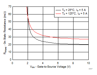
 RDS(on) vs
VGS
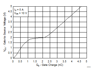
 Gate Charge