SLPS597D April   2017  – June 2024 CSD88599Q5DC

PRODUCTION DATA  

  1.   1
  2. 1Features
  3. 2Applications
  4. 3Description
  5. 4Specifications
    1. 4.1 Absolute Maximum Ratings
    2. 4.2 Recommended Operating Conditions
    3. 4.3 Power Block Performance
    4. 4.4 Thermal Information
    5. 4.5 Electrical Characteristics
    6. 4.6 Typical Power Block Device Characteristics
    7. 4.7 Typical Power Block MOSFET Characteristics
  6. 5Application and Implementation
    1. 5.1 Application Information
    2. 5.2 Brushless DC Motor With Trapezoidal Control
    3. 5.3 Power Loss Curves
    4. 5.4 Safe Operating Area (SOA) Curve
    5. 5.5 Normalized Power Loss Curves
    6. 5.6 Design Example – Regulate Current to Maintain Safe Operation
    7. 5.7 Design Example – Regulate Board and Case Temperature to Maintain Safe Operation
    8. 5.8 Layout
      1. 5.8.1 Layout Guidelines
        1. 5.8.1.1 Electrical Performance
        2. 5.8.1.2 Thermal Considerations
      2. 5.8.2 Layout Example
  7. 6Device and Documentation Support
    1. 6.1 Receiving Notification of Documentation Updates
    2. 6.2 Support Resources
    3. 6.3 Trademarks
    4. 6.4 Electrostatic Discharge Caution
    5. 6.5 Glossary
  8. 7Revision History
  9. 8Mechanical, Packaging, and Orderable Information

Typical Power Block MOSFET Characteristics

TJ = 25°C, unless stated otherwise.
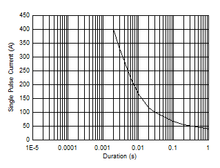
CSD88599Q5DC Single Pulse Current vs Pulse Duration
Max RθJA = 125°C/W
Figure 4-7 Single Pulse Current vs Pulse Duration
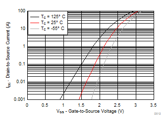
CSD88599Q5DC MOSFET Transfer Characteristics
VDS = 5V
Figure 4-9 MOSFET Transfer Characteristics
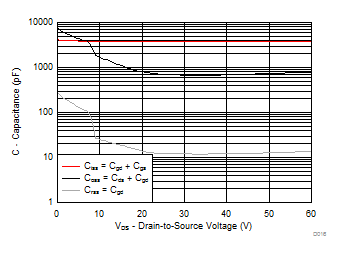
CSD88599Q5DC MOSFET Capacitance
Figure 4-11 MOSFET Capacitance
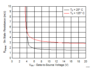
CSD88599Q5DC MOSFET RDS(on) vs VGS
ID = 30A
Figure 4-13 MOSFET RDS(on) vs VGS
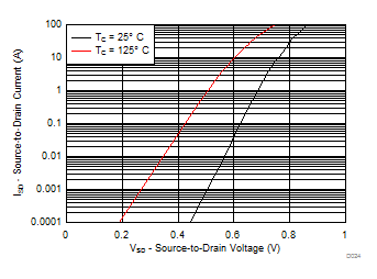
CSD88599Q5DC MOSFET Body Diode Forward Voltage
Figure 4-15 MOSFET Body Diode Forward Voltage
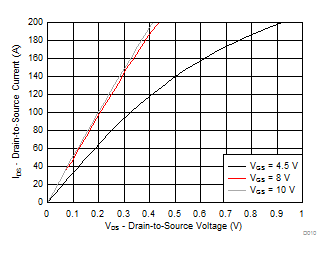
CSD88599Q5DC MOSFET Saturation Characteristics
Figure 4-8 MOSFET Saturation Characteristics
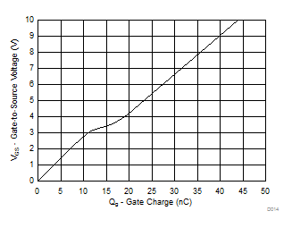
CSD88599Q5DC MOSFET Gate Charge
ID = 30AVDS = 30V
Figure 4-10 MOSFET Gate Charge
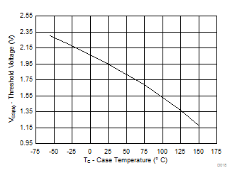
CSD88599Q5DC Threshold Voltage vs Temperature
ID = 250µA
Figure 4-12 Threshold Voltage vs Temperature
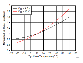
CSD88599Q5DC MOSFET Normalized RDS(on) vs Temperature
ID = 30AVDS = 30V
Figure 4-14 MOSFET Normalized RDS(on) vs Temperature
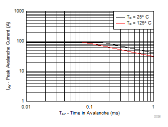
CSD88599Q5DC MOSFET Single Pulse Unclamped Inductive Switching
Figure 4-16 MOSFET Single Pulse Unclamped Inductive Switching