SLPS598E May 2017 – June 2024 CSD88584Q5DC
PRODUCTION DATA
- 1
- 1Features
- 2Applications
- 3Description
- 4Specifications
-
5Application and Implementation
- 5.1 Application Information
- 5.2 Brushless DC Motor With Trapezoidal Control
- 5.3 Power Loss Curves
- 5.4 Safe Operating Area (SOA) Curve
- 5.5 Normalized Power Loss Curves
- 5.6 Design Example – Regulate Current to Maintain Safe Operation
- 5.7 Design Example – Regulate Board and Case Temperature to Maintain Safe Operation
- 6Layout
- 7Device and Documentation Support
- 8Revision History
- 9Mechanical, Packaging, and Orderable Information
6.1.1 Electrical Performance
The CSD88584Q5DC power block has the ability to switch at voltage rates greater than 1kV/µs. Special care must be then taken with the PCB layout design and placement of the input capacitors; high-current, high dI/dT switching path; current shunt resistors; and GND return planes. As with any high-power inverter operated in hard switching mode, there will be voltage ringing present on the switch nodes U, V, and W. Switch-node ringing appears mainly at the HS FET turnon commutation with positive winding current direction. The U, V, and W phase connections to the BLDC motor can be usually excluded from the ringing behavior since they are subjected to high-peak currents but low dI/dT slew-rates. However, a compact PCB design with short and low-parasitic loop inductances is critical to achieve low ringing and compliance with EMI specifications.
For safe and reliable operation of the three-phase inverter, motor phase currents have to be accurately monitored and reported to the system microcontroller. One current sensor needs to be connected on each motor phase winding U, V, and W. This sensing method is best for current sensing as it provides good accuracy over a wide range of duty cycles, motor torque, and winding currents. Using current sensors is recommended because it is less intrusive to the VIN and GND connections.
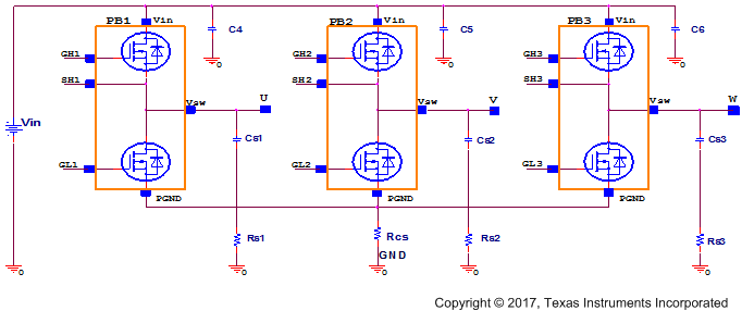
 Figure 6-1 Recommended Ringing Reduction Components
However, for cost sensitive applications, current sensors are generally replaced with current sense resistors.
- For designs using the 60V three-phase smart gate driver DRV8320SRHBR, current sense resistor RCS can be placed between common source terminals for all 3 power block devices CSD88584Q5DC to PGND and measured using an external current sense amplifier as depicted in Figure 6-1 above.
- For designs using the 60V three-phase gate driver DRV8323RSRGZT, three current sense resistors RCS1, RCS2 and RCS3 can be used between each CSD88584Q5DC source terminal to GND and measured by the included DRV8323 current sense amplifiers. The three-phase driver IC should be placed as close as possible to the power block gate GL and GH terminals.
Breaking the high-current flow path from the source terminals of the power block to GND by introducing the RCS current shunt resistors introduces parasitic PCB inductance. In the event the switch node waveforms exhibits peak ringing that reaches undesirable levels, the ringing can be reduced by using the following ringing reduction components:
- The use of a high-side gate resistor in series with the GH pin is one effective way to reduce peak ringing. The recommended HS FET gate resistor value will range between 4.7Ω to 10Ω depending on the driver IC output characteristics used in conjunction with the power block device. The low-side FET gate pin GL should connect directly to the driver IC output to avoid any parasitic cdV/dT turnon effect.
- Low inductance MLCC caps C4, C5, and C6 can be used across each power block device from VIN to the source terminal PGND. MLCC 10nF, 100V, ±10%, X7S, 0402, PN: C1005X7S2A103K050BB are recommended.
- Ringing can be reduced via the implementation of RC snubbers from each switch node U, V, and W to GND. Recommended snubber component values are as follows:
- Snubber resistors Rs1, Rs2, Rs3: 2.21Ω, 1%, 0.125W, 0805, PN: CRCW08052R21FKEA
- Snubber caps Cs1, Cs2, and Cs3: MLCC 4.7nF, 100V, X7S, 0402, PN: C1005X7S2A472M050BB
With a switching frequency of 20kHz on the three-phase inverter, the power dissipation on the RC snubber resistor is 80mW per channel. As a result, 0805 package size for resistors Rs1, Rs2, and Rs3 is adequate.