SLPS598E May 2017 – June 2024 CSD88584Q5DC
PRODUCTION DATA
- 1
- 1Features
- 2Applications
- 3Description
- 4Specifications
-
5Application and Implementation
- 5.1 Application Information
- 5.2 Brushless DC Motor With Trapezoidal Control
- 5.3 Power Loss Curves
- 5.4 Safe Operating Area (SOA) Curve
- 5.5 Normalized Power Loss Curves
- 5.6 Design Example – Regulate Current to Maintain Safe Operation
- 5.7 Design Example – Regulate Board and Case Temperature to Maintain Safe Operation
- 6Layout
- 7Device and Documentation Support
- 8Revision History
- 9Mechanical, Packaging, and Orderable Information
4.6 Typical Power Block Device Characteristics
The typical power block system characteristic curves (Figure 4-1 through Figure 4-6) are based on measurements made on a PCB design with dimensions of 4in (W) × 3.5in (L) × 0.062in (H) and 6 copper layers of 2oz copper thickness. See Section 5 section for detailed explanation. TJ = 125°C, unless stated otherwise.
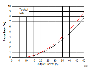
| VIN = 24V | VGS = 10V | D.C. = 50% | ||
| ƒSW = 20kHz | L = 480µH |
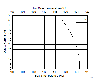
| VIN = 24V | VGS = 10V | D.C. = 50% | ||
| ƒSW = 20kHz | L = 480µH |
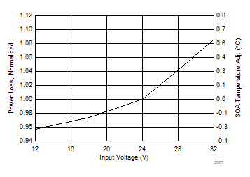
| IOUT = 50A | VGS = 10V | L = 480µH | ||
| ƒSW = 20kHz | D. C. = 50% |
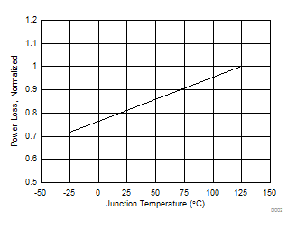
| VIN = 24V | VGS = 10V | D.C. = 50% | ||
| ƒSW = 20kHz | IOUT = 50A | L = 480 µH |
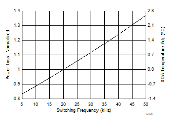
| VIN = 24V | VGS = 10V | L = 480µH | ||
| IOUT = 50A | D. C. = 50% |
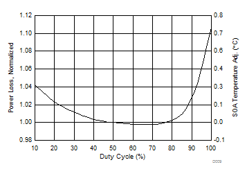
| VIN = 24V | VGS = 10V | IOUT = 50A | ||
| ƒSW = 20kHz | L = 480µH |