SLUAA16A August 2020 – October 2023 BQ79600-Q1
2.4 Daisy Chain Communication
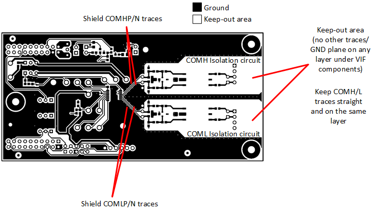
It is important to have proper layout on the COMHP/N and COMLP/N circuits to have the best robust daisy chain communication.
Maintaining signal integrity on the daisy chain communication lines is critical to the success of this part.
- Keep differential traces as short as possible and as straight as possible. Minimize turns and avoid any looping on the traces.
- Keep the differential traces on the same layers. Run the trace in parallel with shielding and matching trace impedance.
- Place the isolation components close to the connectors.
- When using capacitive isolation, place the high voltage capacitor of the COMxP/N pair (where x = H, L) close to each other along the parallel traces.
- Create a keep-out area (no other traces and no ground plane) around the daisy chain components in all PCB layers.
 Figure 2-1 Daisy Chain Layout
Considerations