SLUAA84A January 2021 – February 2022 BQ769142 , BQ76942 , BQ76952
6 Transistor Driver Implementation
While an IC FET driver is very capable, there are instances where the user does not need the high performance of the integrated driver and may choose to implement a driver with transistors. The same voltage ranges for the power FET gates must be supported by the circuit. The logic level of the DDSG and DCHG signals must be translated to the higher gate voltage for the power FETs. Many transistor designs are possible. If the input polarity for the transistor drivers are different, adjust the polarity of the DDSG and DCHG in the BQ769x2 configuration as needed. An example test circuit is shown in Figure 6-1. This circuit also uses a simple regulator with a Zener to a NPN emitter follower for the "12 V" driver voltage VFET. R71 and C68 filter transients on the BAT+ to avoid possible coupling to the VFET output. The VFET load is typically small, but select the R71 value and power rating for the continuous and surge currents selected for the design. While the circuit implementation is simple, the 280 uA at 40 V to bias the Zener may lead a designer to a more sophisticated design. The discharge driver uses a single FET Q36 to provide level shifting to the VFET voltage level. Since Q36 inverts the signal, its input is biased high so that the driver is off when VFET voltage is present but the DDSG signal is not configured. DDSG must not go above its ABS MAX of 6 V, so a voltage divider is used. The driver requires a bias current in R74 when the driver is off. The level shifted signal at the Q36 drain drives the FET gates through emitter followers Q34 and Q37. The emitter follower configuration will drive current through the FET switching area but will limit the voltage from reaching the VFET and GND levels.
With the inverted discharge driver the DDSG polarity must be inverted for this driver.
Settings:Configuration:DCHG Pin Config 0x22
The charge driver is noninverting and does not drive low since a blocking diode is used. When DCHG is high Q42 turns on Q41 to provide the VFET voltage for the charge power FET gates. Output current is limited by R102. When DCHG is low Q42 is off, R105 turns off Q41, and the power FET RGS resistor or an additional gate circuit will pull the power FET gate low.
Figure 6-2 shows a single discharge and charge FET circuit structure controlled by the transistor FET driver. The P-channel device Q2 is not included with the FETs since its function is provided by the transistor driver circuit Q41.
CSD19536KCS FETs were used for the testing of the transistor driver circuit. Results for switching the single FETs are shown in Figure 6-3 to Figure 6-6. The ripple in the discharge turn on indicates the layout may be sensitive to this turn on speed and a larger R27 or circuit improvement may be desired.
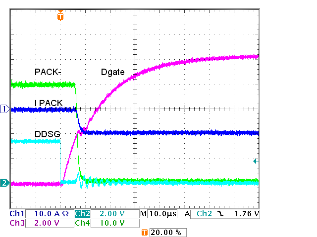 Figure 6-3 Transistor FET Drive, One
Discharge FET, On
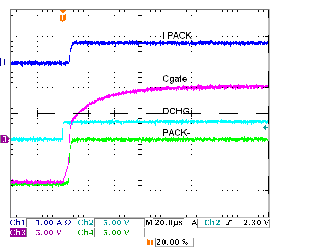 Figure 6-5 Transistor FET Drive, One
Charge FET, On
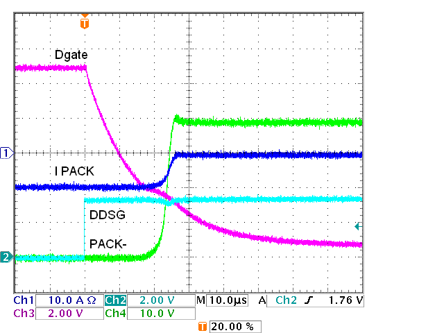 Figure 6-4 Transistor FET Drive, One
Discharge FET, Off
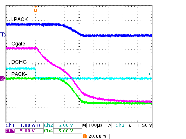 Figure 6-6 Transistor FET Drive, One
Charge FET, Off
Figure 6-6 Transistor FET Drive, One
Charge FET, OffWith many FETs just as with the IC FET driver resistances will need to be reduced to the gate to provide suitable switching. Figure 6-7 shows a test circuit with 12 each discharge and charge FETs used with the transistor driver. The circuit is much like the IC FET driver circuit but Q2 is removed since the transistor charge driver has a P-channel output device. Figure 6-8 to Figure 6-12 show the test results. Figure 6-13 shows the improved switching of reducing R24 to 91 kΩ for faster charge turn off.
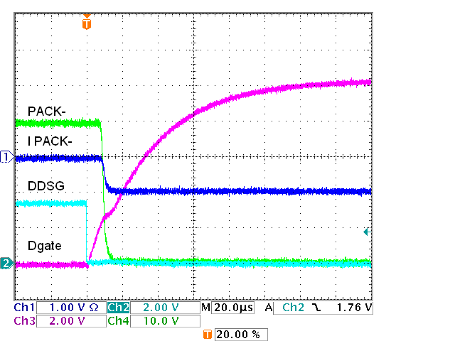 Figure 6-8 Transistor FET Drive, 12 Discharge FETs, On
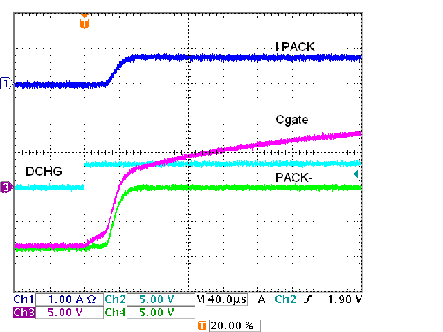 Figure 6-10 Transistor FET Drive, 12 Charge FETs, On, Detail
 Figure 6-12 Transistor FET Drive, 12 Charge FETs, Off, PNP, 1 MΩ
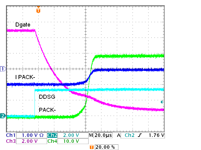 Figure 6-9 Transistor FET Drive, 12 Discharge FETs, Off
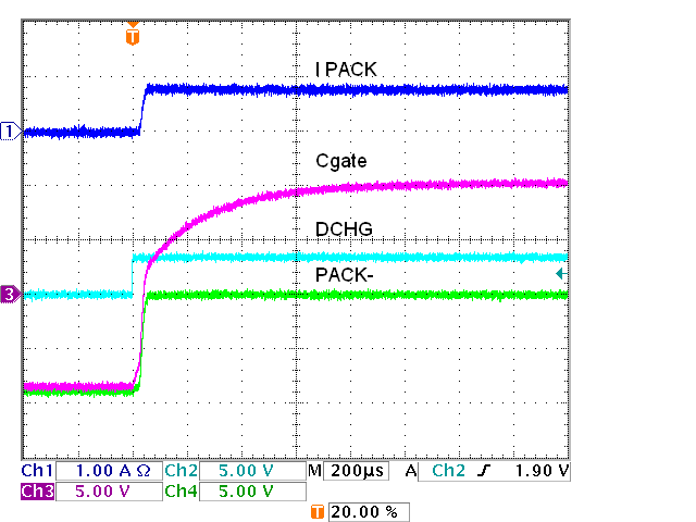 Figure 6-11 Transistor FET Drive, 12 Charge FETs, On
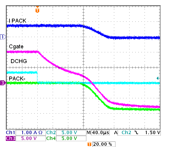 Figure 6-13 Transistor FET Drive, 12 Charge FETs, Off, PNP, 91 kΩ
Again checking the "12 V" VFET supply during switching the 24 FETs on, a dip is observed during turn on as shown in Figure 6-14. The DC level of the "12 V" VFET voltage is below 12 V due to tolerance of the Zener and the base-emitter drop of the transistor Q33.
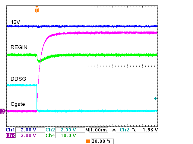 Figure 6-14 12-V Emitter Follower with 24 FETs Turn
On
Figure 6-14 12-V Emitter Follower with 24 FETs Turn
OnThe circuit above has an inverting driver for DSG and biases the input at all times. The emitter follower structure does not drive to the full voltage or GND. Other topologies are possible. Figure 6-15 shows an alternate discharge driver using a push-pull driver. This uses the DDSG polarity high when on and requires bias current on when the driver is on. It does have a shoot through current during switching. In this case switching is infrequent and shoot through current is limited by R101. Example switching of two discharge FETs is shown in Figure 6-16 and Figure 6-17.
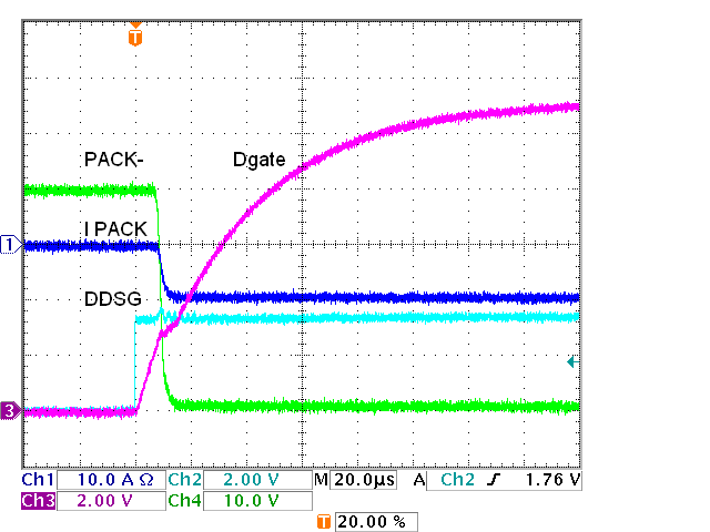 Figure 6-16 Transistor FET Drive, Two Discharge FETs,
On
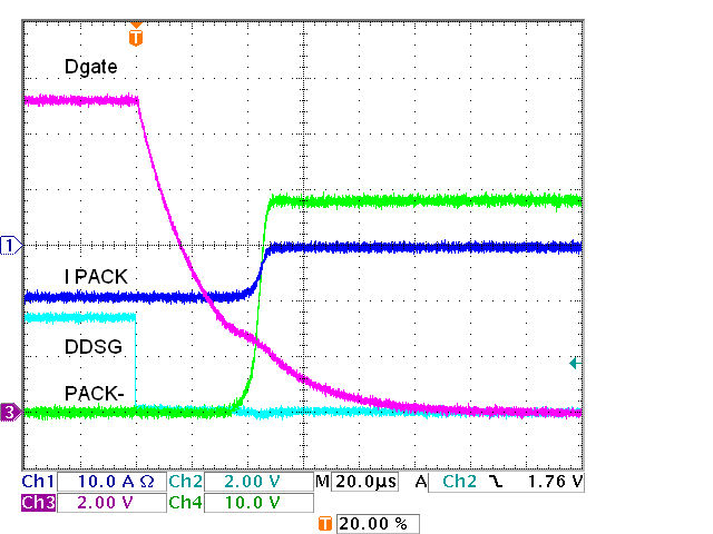 Figure 6-17 Transistor FET Drive, Two Discharge FETs,
Off
Figure 6-17 Transistor FET Drive, Two Discharge FETs,
OffThe load of the driver on the "12 V" VFET can be observed at the filtered input Regin. Shoot through current of the alternate driver is provided by the capacitors and is not apparent in the waveforms of Figure 6-18 and Figure 6-19.
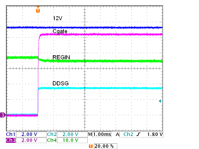 Figure 6-18 12-V with Push-Pull Driver Turn On
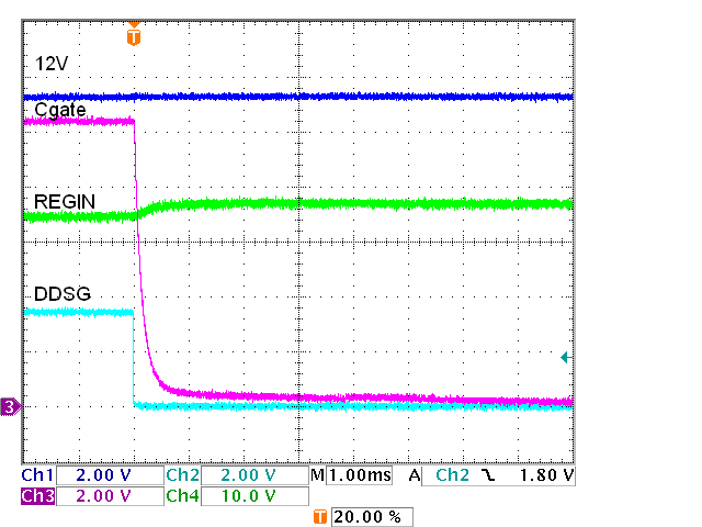 Figure 6-19 12-V with Push-Pull Driver Turn Off