SLUAAH3 October 2021 UCC28056
- Trademarks
- 1How to Select the Correct Devices Version of UCC28056 Families?
- 2How to Complete the Schematic Review of the UCC28056?
- 3How to Test and Confirm the UCC28056 Working Mode?
- 4Protections and how to Identify Them?
-
5Application Debug Frequently Asked Questions
(FAQs).
- 5.1 How is the UCC28056 GND Pin Connected?
- 5.2 There is CCM Inductor Current During Start-Up, is This a Normal Phenomenon?
- 5.3 How to Fine-Tune the RC Parameter on the ZCD/CS Pin?
- 5.4 Is it Possible to Increase the High Voltage Cap Value on the ZCD Cap Divider?
- 5.5 How to Separate the TONMAX Limit or OCP Protection When the PFC Output Voltage Cannot Follow the Regulated Voltage?
- 5.6 Does UCC28056 Support DC Input Application?
- 5.7 How Does RDG Change the Delay Time for Valley Switching Detection of the MOSFET?
- 5.8 Can UCC28056 Meet Harmonic Performance?
- 5.9 Does UCC28056 Have Soft Start?
- 5.10 Does the UCC28056 Support Auxiliary-Winding PFC Inductor Input on the ZCD Pin?
- 6References
2.3 DRV Pin
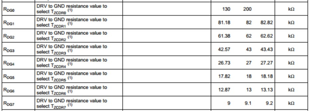
At light load condition when the controller is working at Discontinuous Current Mode (DCM), it is better to turn on the switching MOSFET when drain voltage is at its minimum voltage level to achieve a maximum efficiency. An external resistor connected from DRV to GND adjusts the delay between the drain waveform falling below VIN and the DRV rising edge, allowing the turn on transition to be aligned to the valley minimum accurately over a wide range of idle ring oscillating frequency. Different resistor values of RDG set eight different delay times(TZCDR0 – TZCDR7).
Fine-tune the RDG value for a given switching MOSFET and PFC inductor. Figure 2-2 and Figure 2-3 list the resistor values and the delay times as shown in the data sheet.

Figure 2-2 Eight Different RDG Resistors Settings

Figure 2-3 Eight Different TZCDR Delay Times