SLUAAL6 august 2023 TPS51383 , TPS51386
4 Fast Load Transient Response with D-CAP3 and D-CAP2 Control
Since the load profile can change dramatically in Notebook and Desktop PC applications, it is important to consider AC transient performance. Choosing a DC/DC converter with a fast transient response using non-linear control techniques, such as constant on-time or D-CAP3™, allows a fast transient response with minimal output capacitance. A converter using D-CAP3 control mode has three primary considerations for deciding the value of the output capacitance: transient (which includes load step and slew rate of the load step) output ripple, and stability.
In applications where the load transient is stringent, the output capacitance is predominantly driven by the transient requirement. For a D-CAP3 based design, there is a minimum capacitance requirement in terms of small signal stability. This requirement prevents subharmonic, multiple-pulsing behavior in the modulator.
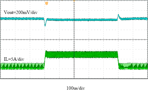
Figure 4-1 shows the transient performance of the 8-A TPS51383 with a 3.3-V output, less than 300mV overshoot, and less than a 30µs recovery with output capacitance of 4x22 µF. The 0.8-A to 7.2-A load step has a slew rate of 2.5-A/µs.
 Figure 4-1 TPS51383 Transient Waveform
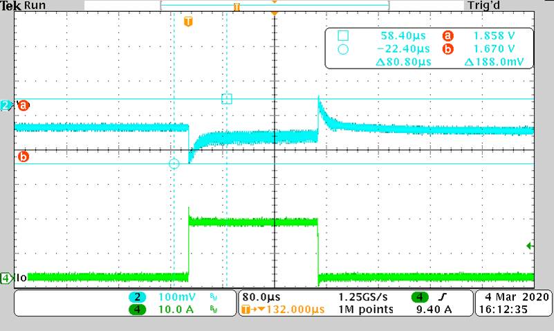
The TPS51215A supplying VCCIN_AUX features adaptive on-time D-CAP2™ control allowing ceramic output capacitors and achieves a fast load transient response shown in Figure 4-2 under the noted conditions below the waveform. The over-voltage and under-voltage test results also meet the target design specification, and the results are shown in Table 4-1 under the same conditions as the TPS51215A load transient waveform. The TPS51215A waveform conditions are VIN=12.6V, slew rate=12A/µs, FSW =600kΩ, L=0.22µH, and COUT=220µF + 22*12µF.
 Figure 4-2 TPS51215A Load Transient Waveform
| Voltage Rail | Type | Load Transient | Validation Result (V) | Target (V) |
|---|---|---|---|---|
| 0.8 V | Undershoot | 0 A to 16 A | 1.67 | 1.62 |
| Overshoot | 16 A to 0 A | 1.858 | 1.89 | |
| 1.8 V | Undershoot | 17 A to 29 A | 1.678 | 1.62 |
| Overshoot | 29 A to 17 A | 1.882 | 1.89 |