SLUAAR2 august 2023 BQ27Z746
3 Reverse Charge Protection Without Optional RCP Circuit
The DSG pin should be able to transition to negative voltage when reverse charging connection has occurred. It will drive any voltage across the RCP resistor to 0, turning off the DFET, and protecting the battery from discharging. Figure 3-1 shows a system diagram of BQ27Z746 for reverse charge protection. It shows that BQ27Z746 has an internal P channel MOSFET. The PFET blocks the negative voltage from reaching inside the IC with an ESD diode. The ESD diode prevents the pin voltage from going negative. The internal PFET allows the DSG pin voltage transition to negative below ground. If RCP has occurred, PFET will be very slightly turned on with extremely low leakage current. Thus, most reverse voltage is applied across the PFET, and the voltage drop across RGS resistor will be almost 0 V.
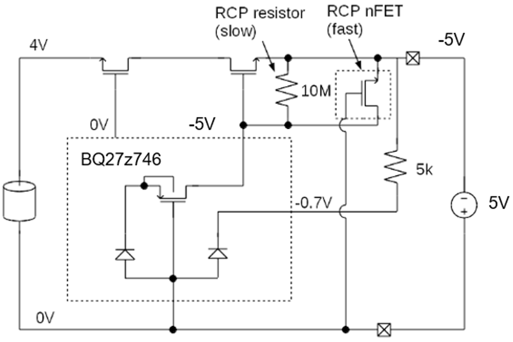 Figure 3-1 Reverse Charger Protection System Diagram
Transition from 0 V to reverse charger voltage (for example, -5 V) occurs via RCP resistor. Equalization time is determined by the resistance value and gate to source capacitance of discharging FET. With 10 MΩ resistance and 2 nF capacitance, the equalization time is approximately 50 ms. Figure 3-2 shows the simulation model for this operation with TINA. Figure 3-3 and Figure 3-4 shows the simulation results based on the resistance value. With 5 MΩ resistance value, the transition to negative of DSG pin is 2x faster than 10 MΩ resistance value. However, lowering the resistance value will increase the current consumption of the device in normal operation by increasing the output current load on the charge pump. Demand for fast equalization time can be determined by the current of the reverse charger voltage source.
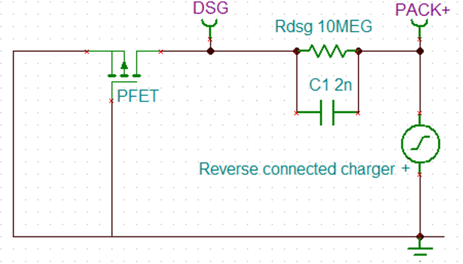 Figure 3-2 Simulation Model for Internal RCP Circuit of BQ27Z746
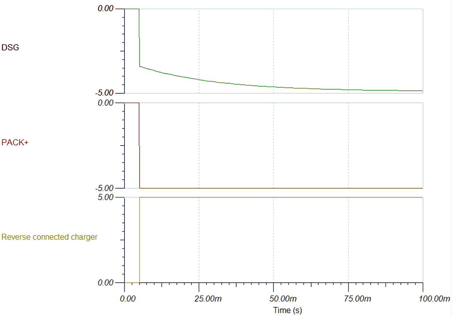 Figure 3-3 Simulation Result When RGS = 10 MΩ
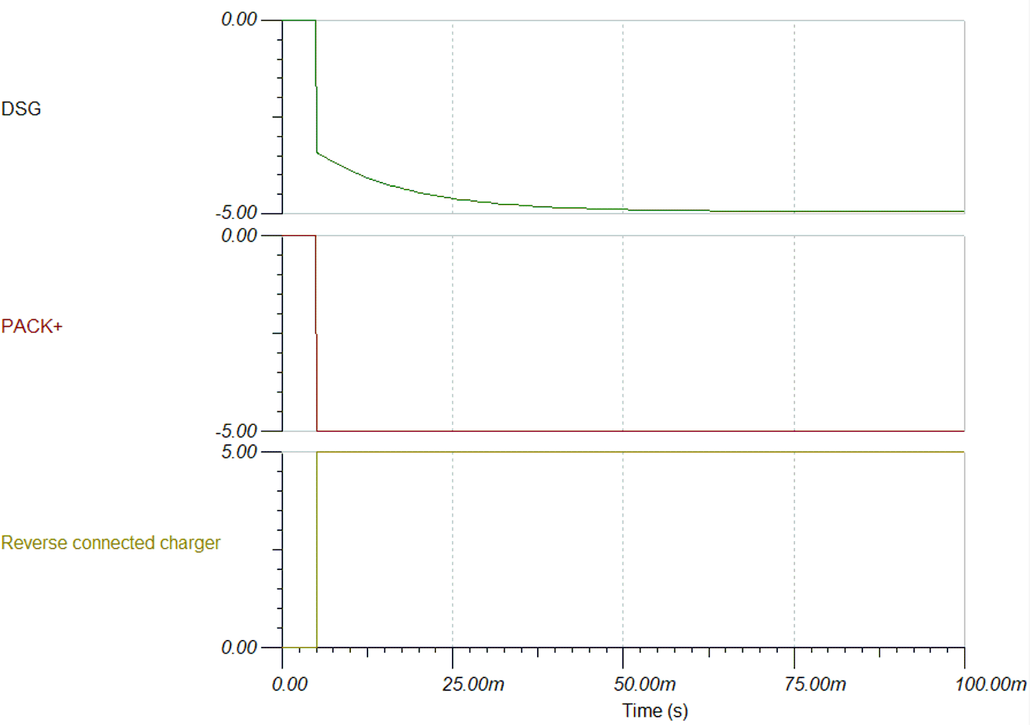 Figure 3-4 Simulation Result When RGS = 5 MΩ
Figure 3-5 shows the waveform when reverse charger connection has occurred using a gauge which does not have an internal RCP circuit. The battery charger source has limited charging current to 200 mA as reference. Therefore, the battery discharging current is 200 mA in the waveform. The battery discharging current will get as high as the reverse connected source's current limit. Figure 3-6 shows the waveform when reverse charge connection is occurred with BQ27Z746 without optional RCP circuit. The power source limited charging current to 3 A. As a result, BQ27Z746 successfully protects discharging current from battery. At this measurement, DSG pin was not connected to oscilloscope. Since a probe can connect the RCP resistor to ground on DSG, the DSG pin cannot transition negative if there is a 10 MΩ from DSG to ground through the scope connection.
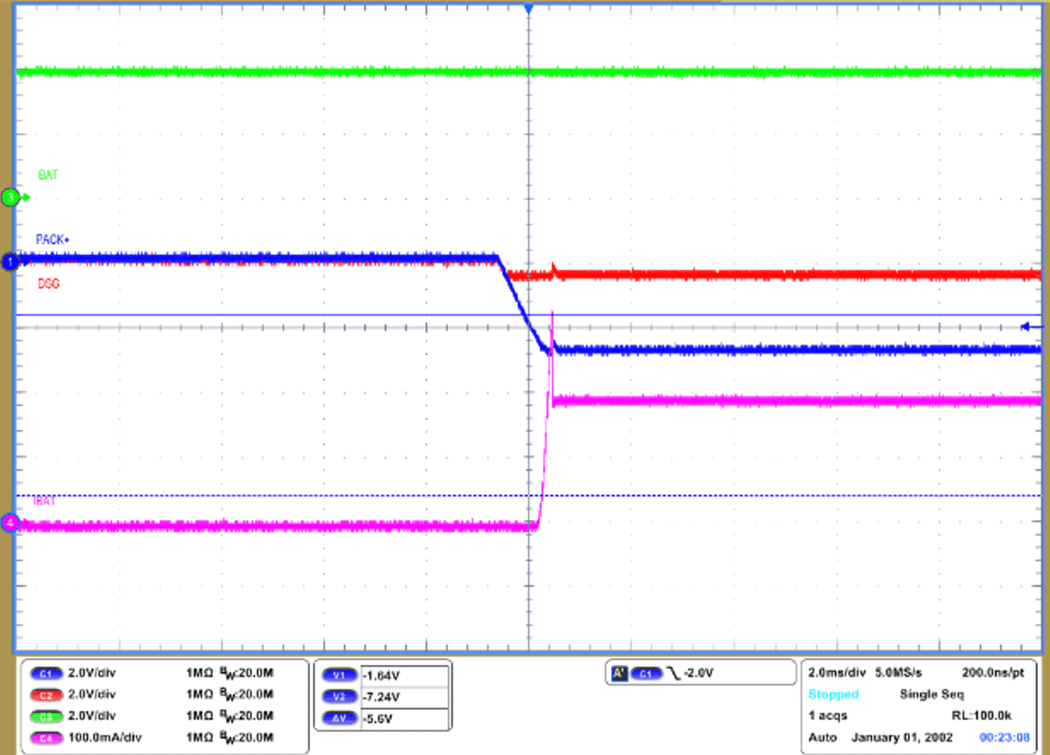 Figure 3-5 Reverse Charge Connection With the Gauge Which Does Not Have Internal RCP
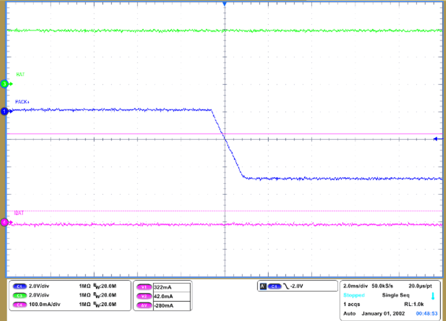 Figure 3-6 Reverse Charge Connection with BQ27Z746 which has internal RCP
Figure 3-7 shows the placement of optional RCP circuit in PCB from BQ27Z746 reference schematic. With BQ27Z746, User can save 27 mm2 of PCB size and BOM cost by removing the components of optional RCP circuit.
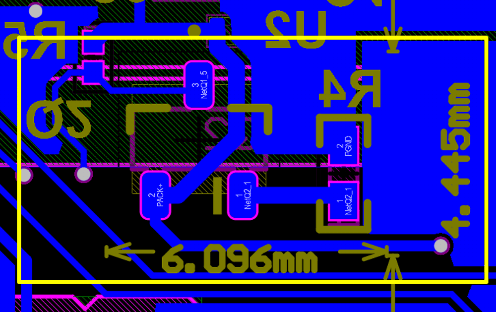 Figure 3-7 Optional RCP Circuit in PCB