SLUAAT6 July 2024 BQ41Z50
2.1 Cell Voltage Calibration
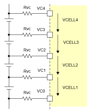
Figure 2-1 illustrates cell voltage calibration.
 Figure 2-1 Cell Voltage Calibration
- Apply known voltages in mV to the
cell voltage inputs:
- VCELL1 between VC1 pin and VSS pin
- VCELL2 between VC2 pin and VC1 pin
- VCELL3 between VC3 pin and VC2 pin
- VCELL4 between VC4 pin and VC3 pin
- If ManufacturerStatus()[CAL] = 0, send 0x002D to ManufacturerAccess() to enable the [CAL] flag.
- Send 0xF081 or 0xF082 to ManufacturerAccess() to enable raw cell voltage output on ManufacturerData().
- Poll ManufacturerData() until the 8-bit counter value increments by 2 before reading data.
- Read the ADC conversion readings
of cell voltages from ManufacturerData():
ADCCELL1 = BBbb of ManufacturerData()
Is ADCCELL1 < 0x8000? If yes, use ADCCELL1; otherwise, ADCCELL1 = –(0xFFFF – BBbb + 0x0001).
- Average several readings for
higher accuracy. Poll ManufacturerData() until ZZ increments, to indicate
that updated values are available:
ADCCELL1 = [ADCCELL1(reading n) + … + ADCCELL1(reading 1)]/n
-
Average all of the cells to create a single cell gain with the average all voltages:
Equation 1. - Write the new Cell Gain value to data flash.
- Re-check voltage readings and if these are not accurate, repeat steps 4 – 8.
- Send 0x002D to ManufacturerAccess() to clear the [CAL] flag if all calibration is complete.