SLUAAU4 June 2024 UCC28750
2 Retrofit Items
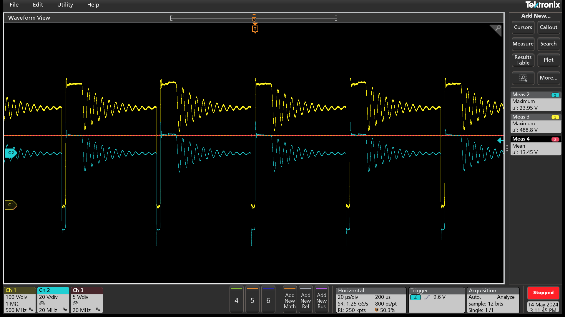
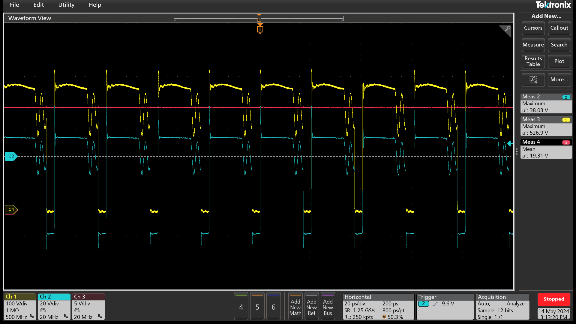
The Auxwinding voltage reflects the VDS waveform, so the VDS voltage spike also impacts the VDD voltage. The VDS voltage spike is increased when output loading increased too, so the VDD voltage is charged higher at full load.
That is why the RCD snubber is increased and also adds additional snubber at Auxwinding, so the snubber can avoid IC to trigger VDD OVP at heavy load.
TI also published the Power Tips training video to explain how to fine tune RC snubber.
The Figure 2-2 and Figure 2-3 shows VDS (Ch1) and Vaux(Ch2) and VDD(Ch3) waveform at different loading, and the VDD is increased at higher loading.
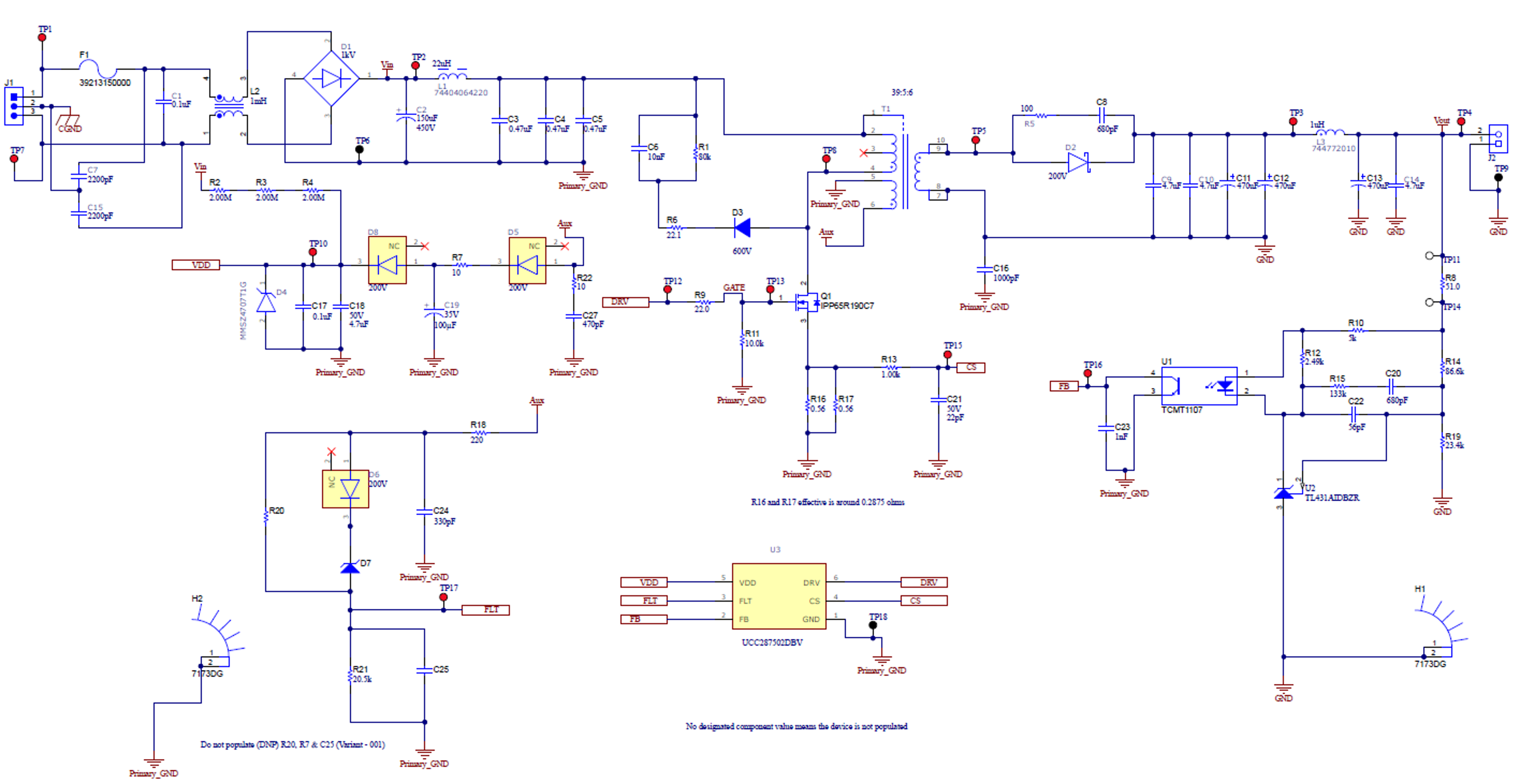
The change is listed in the following:
- Transformer changed to RM10 Bobbin.
- Lm : 660uH ; Lr : 11uH
- Np : Ns : Na = 39 : 5 : 6
- C6 : 10nF
- R1 : 80KΩ
- R7 : 10Ω
- R19 : 23.4KΩ
- R10 : 5KΩ
- add additional RC filter at Auxwinding
- R22 : 10Ω
- C27 : 470pF
 Figure 2-1 Updated Schematic
 Figure 2-2 Output Load at 0.5A; VDD
13.45V
 Figure 2-3 Output Loading at 4A; VDD 19.31V