SLUAAW4 August 2024 UCC57108
Introduction
As electric vehicles grow in popularity, engineers are tasked with designing systems that are efficient and safe for users. One aspect that must be considered for hybrid electric (HEV) and full electric (EV) vehicle architectures is the traction inverter. Typically, in HEV architectures, a three-phase inverter is used to drive the electric motor of a vehicle. The inverter design largely depends on the overall power requirements of the system, and what type of architecture is used overall for the HEV architecture. An internal combustion engine is involved with an HEV architecture, but this is not the case for EVs. Therefore, inverters require different energy sources depending on the vehicle architecture type. Regardless, the traction inverter plays an important role in driving electric motors in both HEV and EV systems.
Many elements are involved in a traction inverter system architecture, including the power management stage, high-power switches, and the microcontroller used to control the gate drivers. SiC (Silicon carbide) MOSFET (metal-oxide semiconductor field effect transistor) or IGBT (insulated-gate bipolar transistor) switches are commonly used in these systems. The switches are crucial in the inverter operation, as the inverter allows the current to flow to the electric motors and allow for motion of the vehicle. Since switches are very important, many monitors and sensors are included to maintain correct operation of the switches, such as temperature, voltage, and current sensing. Furthermore, with the long list of possible fault scenarios, detecting faults as quickly as possible is important for engineers.
Desaturation Protection
Desaturation protection, a popular method to detect a short-circuit fault, is integrated into the UCC5710x-Q1. UCC5710x-Q1 is Texas Instruments’ first non-isolated gate driver with integrated protection features, shown in Figure 1.
 Figure 1 Pinout for the UCC57108B-Q1 in
the D package.
Figure 1 Pinout for the UCC57108B-Q1 in
the D package.Desaturation detection, or DESAT, is a popular way to monitor IGBT or SiC MOSFET behavior. DESAT monitors the voltage across the switch being used when the switch is turned on. If a fault, such as a short circuit occurs, DESAT can detect the rise in voltage (Vce or Vds) due to the extreme rise in current across the switch. When the voltage surpasses a fault detection threshold voltage (which is based on the gate driver and power switch used), the DESAT protection is activated and the output of the driver is turned off to protect the switch from catastrophic breakdown during a fault.
An example DESAT fault-protection circuit consists of a resistor, blanking capacitor, and a diode, as shown in Figure 2. During normal operation, the diode is forward biased, allowing the current to flow through the diode and preventing the blanking capacitor from charging. In a short circuit event, the voltage across the switch rises and reverse biases the diode, allowing current to flow through the blanking capacitor. After a time set by the capacitance value, the voltage on the capacitor exceeds the internal DESAT threshold voltage and a DESAT is detected.
 Figure 2 Desaturation Detection
Circuit.
Figure 2 Desaturation Detection
Circuit.UCC5710x-Q1 features a built-in DESAT detection circuit, where the detection time is programmable by the external components. The timing is controlled by CBLK and the time to charge the capacitor is called the blanking time, which can be calculated as:
UCC5710x-Q1 features a typical 150ns internal leading edge blanking time after the input switches to a high state. During the blanking time period, the gate driver avoids false triggers, such as noise generated during turn-on transitions. After this internal leading edge blanking time, an internal current source ( ) is activated to charge the external blanking capacitor, where the typical value of the current source is 250µA for the 250µA variant of UCC5710x-Q1. This gate driver has a typical DESAT pin threshold of 6.5V but can be adjusted externally by adding more DHV diodes in series or by adding a Zener diode in series. Another method to adjust the DESAT threshold voltage is to change the value of the resistor, though this must not be used for adjustments larger than a few hundred mV. A Zener diode can be used to make larger adjustments (for example, 3V) and are available in several knee voltages. When selecting a Zener, the voltage drop depends on the current bias, which is in this case. UCC5710x-Q1 offers designers a way to customize the DESAT protection in circuits based on the switches used and the timings required.
Fault Reporting
UCC5710x-Q1 also comes with active low fault reporting. When a DESAT fault is detected, the nFLT pin gets pulled down to GND and is held low until the fault is clear. Figure 3 showcases a DESAT fault occurring, causing the fault pin to pull low to ground, and the output to turn off as well.
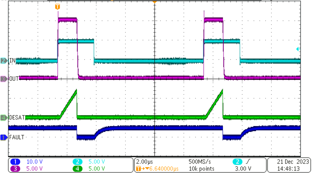 Figure 3 DESAT and Fault Feature of
UCC57108B-Q1
Figure 3 DESAT and Fault Feature of
UCC57108B-Q1The system designer can choose to have this fault signal fed to the microcontroller unit (MCU) or digital signal processor (DSP) that is controlling UCC5710x-Q1 and take action if a fault is detected. Furthermore, the nFLT pin is able to report faults in the internal thermal shutdown (TSD) or a undervoltage lock out (UVLO). If the device experiences a significant increase in temperature, or the supply voltage is lower than UVLO, the fault pin is pulled low to ground, indicating a fault has occurred. UCC57108B-Q1 in the D package has a junction to ambient thermal resistance of 126.4°C/W, meaning that the device has better thermal resistance than some drivers made by competitors. Figure 4 and Figure 5 show the thermal performances of UCC57108B-Q1 and a competitor part for VDD = 15V, 0 to 5V input with a 100kHz switching frequency, and a 1nF load. UCC57108B-Q1 is less sensitive to temperature changes and showcases great thermal capabilities. The fault detection that is incorporated within the UCC5710x-Q1 allows engineers to monitor faults that occur when the system is running, and can protect systems from potential damages.
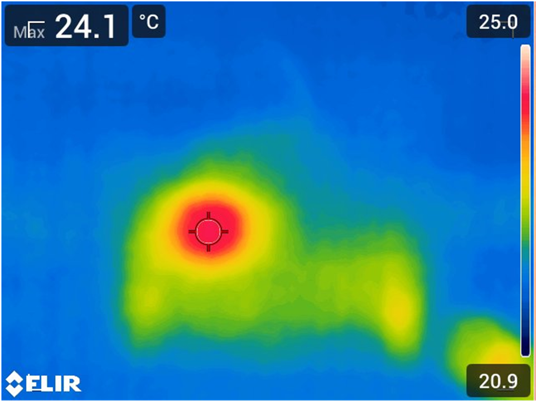 Figure 4 UCC57108B-Q1 Thermal
Testing
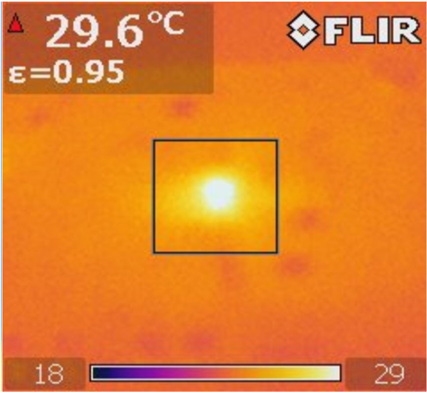 Figure 5 Competitor Thermal
Testing.
Figure 5 Competitor Thermal
Testing.Application
The UCC5710x-Q1 serves as a great high-speed, low-side gate driver with protection features that are beneficial for automotive applications, such as traction inverters, HEV/EV positive temperature coefficient (PTC) heaters, resident EV chargers, and many more. With the protection features of the UCC5710x-Q1, engineers can design a system to detect and protect the overall systems from faults. For example, engineers can track a fault in the traction inverter and have the system respond accordingly with the device. The inputs are capable of withstanding up to -5V and are VDD capable inputs. Having a wide range for the input voltage allows engineers more versatility and robustness; providing for a wider range of signals to enter the device with less concerns.
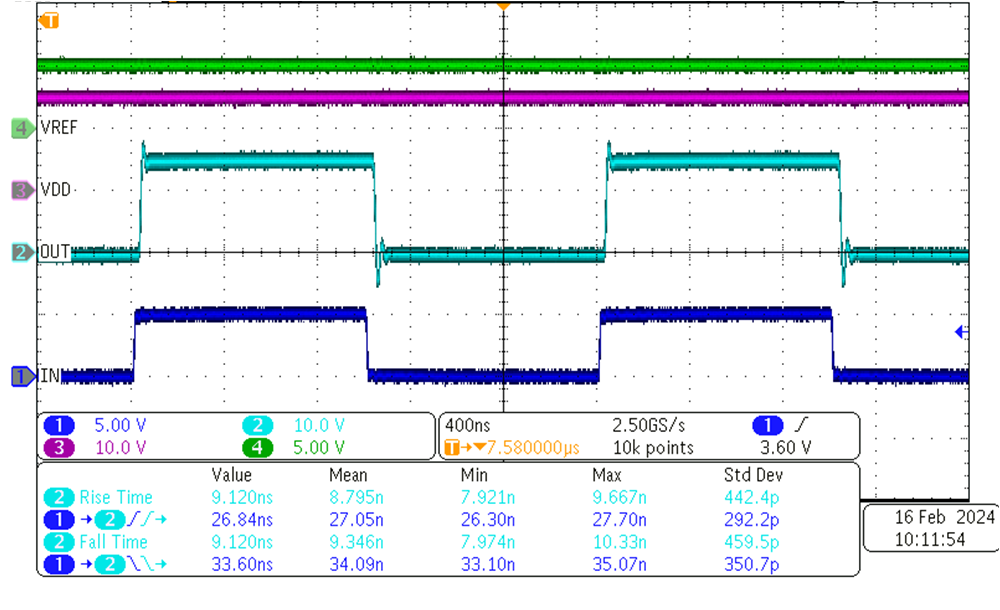 Figure 6 UCC57108B-Q1 Rising and
Falling Propagation Delays
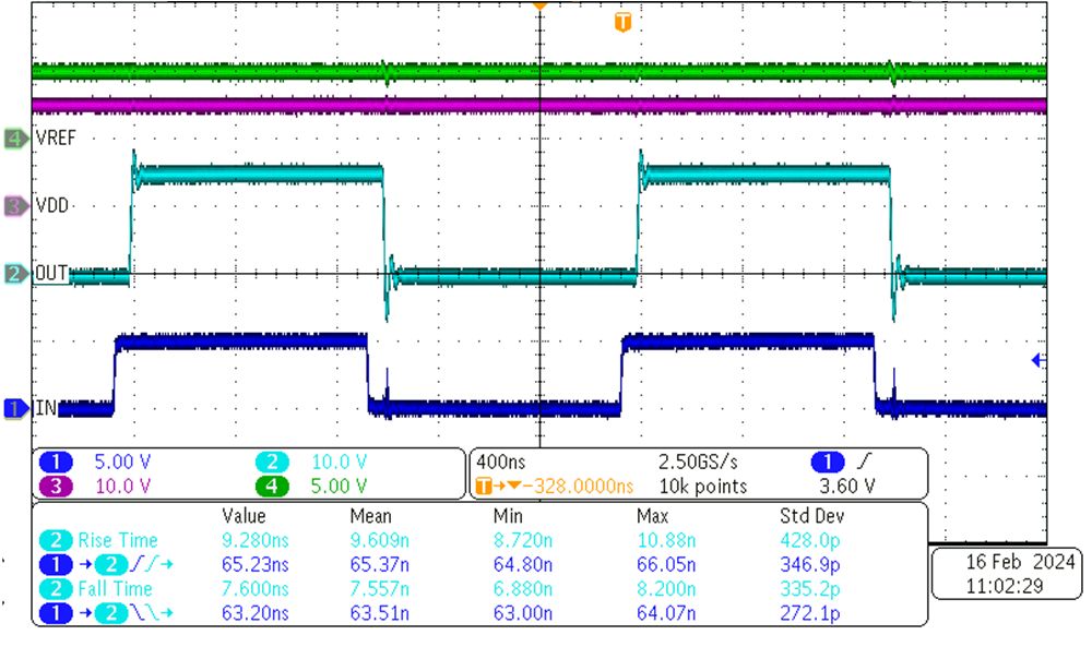 Figure 7 Competitor Rising and Falling
Propagation Delays
Figure 7 Competitor Rising and Falling
Propagation DelaysFurthermore, UCC5710x-Q1 boasts a low propagation delay and a low minimum input pulse width; meaning engineers can take advantage of a device that is faster and more reliable for automotive applications. Figure 6 shows the propagation delay of UCC57108B-Q1 and Figure 7 shows the propagation delay of a competitor device. The devices are running with an input of 0 to 5V with a frequency of 500kHz, driving a 1nF capacitive load with VDD = 15V. The low propagation delay and minimum input pulse width also allows for engineers to have a fast device that can respond to input changes much faster. Table 1 summarizes key differences between UCC57108B-Q1 and a competitor part. UCC5710x-Q1 offers increased system robustness and a better design compared to other gate drivers with a similar pin out and features. UCC5710x-Q1 offers a robust option to automotive designs and allows engineers to create a system that is reliable, fast, and safe.
| Design Considerations | UCC57108B-Q1 | Competitor 1 |
|---|---|---|
|
Positive Power Supply (VDD-GND) Absolute Maximum |
30V | 22V |
|
Input Signal DC Voltage Absolute Maximum |
30V | 5.5V |
|
Propagation Delay Falling/Rising Typical |
28ns/26ns | 54ns/59ns |
|
Input Pulse Width Minimum Passed to Output |
9ns | 40ns |
|
Junction-to-ambient Thermal Resistance (RθJA) |
126.4°C/W | 176°C/W |
References
- Texas Instruments, Understanding the Short Circuit Protection for Silicon Carbide MOSFETs, application brief.
- Texas Instruments, HEV/EV Traction Inverter Design Guide Using Isolated IGBT and SiC Gate Drivers, application note.
- Texas Instruments, UCC5710x-Q1 High-Speed, Low-Side Gate Drivers With DESAT Protection For Automotive Applications, data sheet.
- Texas Instruments, EVM User's Guide: UCC57108EVM UCC57108 Evaluation Module, evaluation module user's guide.