SLUP408 February 2022 LM25149-Q1 , LM61460-Q1 , LM61495-Q1 , LMQ61460-Q1
The electrification of everything has introduced electronics to many applications in the world around us. Communications, transportation, factory automation and control, personal electronics, and health care are the most recognizable examples of electronics integration, while software innovation relies on the underlying hardware infrastructure.
With more electronic and computer systems used in smaller and tighter spaces, EMI becomes an increasing focus for system design. Switched-mode power supplies (SMPSs) are the most efficient way to power electronic systems, but they generate a significant amount of EMI. Increased switching speeds and switching frequencies result in higher power density but also tend to make EMI worse.
EMI occurs when electric or magnetic fields couple and interfere between two or more electronic devices or systems. In an electronic system, voltage ripple can result in conducted noise propagating from one circuit to another, especially when there are shared connections such as power-supply rails.
In a simple example, imagine hearing audible noise in a radio system that goes away when removing or replacing a faulty device. That device could have been generating ripple, causing interference within the audible range and coupling to the audio output.
In a broader sense, EMI is not limited to audible noise and can interfere with power, system inputs, processing and system outputs. International EMI standards such as Comité International Spécial des Perturbations Radioélectriques (CISPR) 25 specify EMI amplitude limits for different frequencies [1]. In Figure 2-1, conducted noise amplitude is represented on the Y axis in decibel microvolts; frequency is represented on the X axis in megahertz. The graph plots CISPR 25 noise-limit lines with peak-level detector limits in red and average levels in blue. Noise detected using a specific test setup and equipment specified by the CISPR standard must remain below these limit lines.
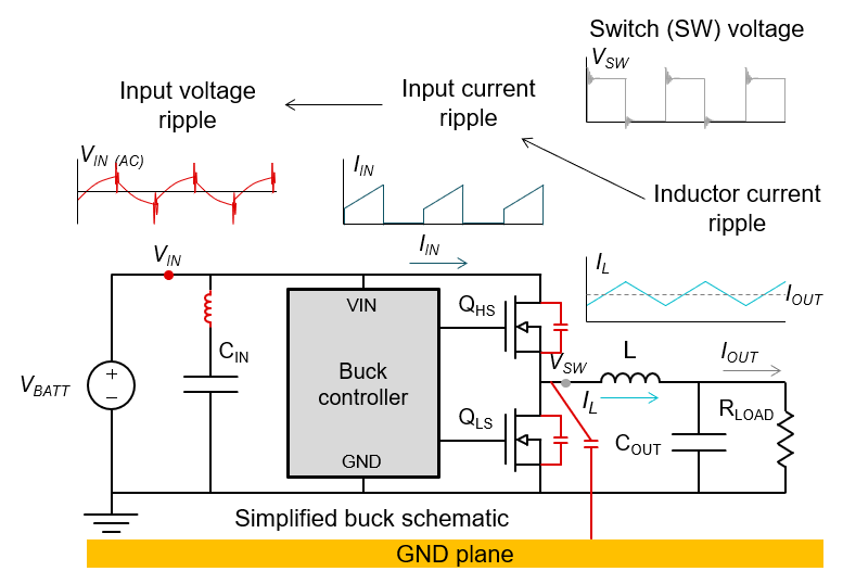
In battery-powered systems (see Figure 3-1), a switched-mode power supply like a buck converter commutates a switch node between a low voltage (GND) and an input voltage. Filtering the switch-node voltage generates an average DC output voltage, which is between the input voltage and GND in the case of a buck converter. The switching causes input ripple at the fundamental switching frequency, and the square edges result in higher-frequency harmonics. Sharper edges with faster slew rates generate higher-frequency harmonic energy. The trapezoidal input current ripple is discontinuous and exhibits the same high-frequency components in the current ripple.
Parasitic capacitances and inductances are nonideal properties of components in the circuit. These parasitics interact negatively with the voltage and current and generate very-high-frequency spikes and ringing noise. On the other hand, jitter and dithering (spread spectrum) can create low-frequency oscillation and noise. Figure 3-2 shows common frequency ranges where noise occurs from these sources.
This document discusses advanced power-converter features that improve upon existing methods to further reduce EMI. The five features entail the use of:
Figure 4-1 illustrates how to mitigate and filter EMI with passive components.
A high-frequency ceramic input capacitor helps supply the power metal-oxide semiconductor field-effect transistors (MOSFETs) with high-frequency energy to improve the switch’s slew-rate and edge characteristics, thus reducing switch ringing and high-frequency noise. Bulk capacitance provides low-frequency damping and prevents resonance between the filter components. A capacitor-inductor-capacitor (CLC) EMI filter, also known as a π filter, filters differential-mode noise from 10 MHz to 100 MHz, depending on the components selected.
Other components include a ferrite bead that provides high differential-mode impedance at very high frequencies. The ferrite bead impedance is typically specified at 100 MHz. A common-mode choke filters common-mode noise that usually occurs at high frequencies (10 MHz to 300 MHz).
Conventional CLC EMI filters use a capacitor and inductor arranged as a low-pass filter to attenuate noise from a noisy node to a quiet node. You can design the CLC components based on the required attenuation. Many tools are available to aid in designing filters, including application notes [2] and spreadsheet tools [3], as shown in Figure 4-2.
Alternatively, you could use Equation 1 to measure or estimate the required attenuation:
where fSW is the switching frequency, CIN is the input capacitance, D is the duty cycle, IDC is the converter-inductor DC current and VMAX is the decibel microvolt (dBµV) limit at the switching frequency.
Looking again at Figure 4-2 and considering the filter inductor (LIN) and filter capacitor (CF), the CLC π filter provides 40 dB of attenuation per decade at frequencies above the cutoff frequency. Figure 3-1 takes the attenuation required at the switching frequency to design the π-filter cutoff frequency:
You can then use Equation 3 to select filter components based on the required cutoff frequency:
After selecting a typical LIN range between 0.1 µH and 10 µH, you can calculate the required CF value. Increasing the capacitance value – as opposed to using larger inductance values, since a larger inductance tends to increase the overall filter size – lowers the cutoff frequency. Plus, higher-value inductors tend to have decreased current ratings for a given size. The most space-efficient designs use more parallel capacitors rather than a larger inductor value.
Increasing CF capacitance with multiple parallel capacitors is usually easier and more space-effective than increasing LIN to adjust the filter cutoff frequency. Furthermore, a higher inductance will have a decreased current rating for given size.
CF connects to the main power rail and must be rated for the maximum DC voltage. Designs requiring a large CF and a higher DC voltage will necessitate the use of a larger and more expensive capacitor. Similarly, LIN must be rated for the maximum input current (IIN) at minimum input voltages. In higher-power systems, the inductor size and cost will further increase given the larger inductance and DC current requirements. Transients such as load dump and cold crank exacerbate the VIN and IIN requirements.
A second-order effect is that the self-resonant frequency (SRF) decreases as the size of CF increases. At the SRF, the impedance of the equivalent series inductance (ESL) equals that of the capacitance and marks the lowest impedance point over the frequency range. A higher ESL deteriorates the filter’s performance and its ability to attenuate noise at high frequencies.
Figure 5-1 shows two capacitors where the larger capacitor (in blue) is less effective at higher frequencies compared to the smaller capacitor (in black). The figure shows both the impedance and effective capacitance. At frequencies above the SRF, the capacitance rolls off and the parasitic inductance dominates the capacitor impedance. A similar SRF effect can limit LIN in filter performance, where parasitic capacitance dominates the inductor and deteriorates performance at high frequencies.
An AEF uses an amplifier circuit to sense noise on the input rail and inject an out-of-phase signal to cancel the noise being sensed. As shown in Figure 6-1, an operational-amplifier (op-amp) network acts effectively to replace a passive capacitor (CF) with an active capacitor. The op-amp network requires feedback and compensation components, but these components are much smaller in size and cost than a large passive CF. Integrating the op amp into a DC/DC controller package, as in the LM25149-Q1, results in a smaller overall filter size when compared to a fully passive EMI filter.
Figure 6-2 shows a more detailed view of an AEF circuit. An AEF with voltage sensing and current injection (VSCI) uses capacitive sensing and injection; therefore, it does not source or sink any DC current. The AEF cancels the AC ripple current of the input filter inductor (as illustrated in Figure 6-2, with triangular waveforms for simplicity). Consequently, the DC input current does not determine the size of the AEF; instead, it is limited by the op amp’s source-and-sink current capability, as it cancels the AC ripple current in the filter inductor. As a result, an AEF can work with high levels of DC power, with appropriate sizes of LIN and CIN to keep the input ripple and noise within the range of the op amp’s source-and-sink current capability.
The op amp forms a band-stop filter. The term GOp expresses the gain of the op amp, approximated by the active EMI sensing and compensation capacitors CSEN and CAEFC in Equation 4:
Equation 5 has the same format as Equation 3; however, CF is replaced with an injection capacitor (CINJ) and GOp. Using an AEF, you can design for a similar filter cutoff frequency or performance using much lower component values for LIN and CINJ.
For example, with GOp equal to 100, an AEF can reduce the inductance of LIN and the capacitance of CINJ by a factor of 10 for each component. Furthermore, a smaller LIN and CINJ will have lower parasitics and much higher SRFs for better high-frequency performance.
Figure 6-3 and Table 6-1 compare passive and active EMI filters. The passive filter layout uses an inductor that has a significantly larger volume. The AEF layout uses smaller and cheaper components while achieving improved filter performance. The op amp is integrated in the controller integrated circuit (IC), not shown in Figure 6-3.
Passive | Active | |
---|---|---|
Cost | $2.71 | $1.70 |
Area | 110.7 mm2 | 55.8 mm2 |
Height | 5.2 mm | 4 mm |
Figure 6-4 shows the EMI performance of the regulator – without a filter, with a passive EMI filter, and with an AEF. The AEF uses smaller components for a 50% area reduction, with improved EMI attenuation.
It is important to carefully select active EMI components, as some components can cause resonances if you do not meet certain frequency requirements. A sensing or injection component SRF that is less than the active EMI system crossover frequency can create unintended resonance, as shown in Figure 6-5. To avoid resonances, it is recommended to have an active EMI network crossover of around 15 MHz set by input compensation resistor and capacitance RINC and CINC, and using components with an SRF of at least 15 to 20 MHz.
Component layout is an important consideration for AEFs. Keep loop areas formed by circuits small and away from noise sources, and connected directly to a ground plane where large currents are not flowing. At the op-amp IC, place the VCC decoupling capacitor very close to the VCC and power GND pins. Ensure that the AEF amplifier is grounded directly to the ground plane where high currents are not flowing. Keeping the loop area small, route the SEN and INJ traces tightly together from the amplifier.
As shown in Figure 6-6, the SEN and INJ traces should connect directly at compensation components RAEFC, CAEFC and RAEFDC in the blue square. Place the sensing CSEN close to the compensation and the injection-damping network RDAMP, CDAMP and CINJ on the opposite side of sensing, as shown in the red and yellow squares. Finally, be sure that the input compensation CINC and RINC connect to quiet GND, as shown in the purple squares.