SLUS458I July 2000 – June 2024 UCC28C40 , UCC28C41 , UCC28C42 , UCC28C43 , UCC28C44 , UCC28C45 , UCC38C40 , UCC38C41 , UCC38C42 , UCC38C43 , UCC38C44 , UCC38C45
PRODUCTION DATA
- 1
- 1 Features
- 2 Applications
- 3 Description
- 4 Device Comparison Table
- 5 Pin Configuration and Functions
- 6 Specifications
-
7 Detailed Description
- 7.1 Overview
- 7.2 Functional Block Diagram
- 7.3
Feature Description
- 7.3.1 Detailed Pin Description
- 7.3.2 Undervoltage Lockout
- 7.3.3 ±1% Internal Reference Voltage
- 7.3.4 Current Sense and Overcurrent Limit
- 7.3.5 Reduced-Discharge Current Variation
- 7.3.6 Oscillator Synchronization
- 7.3.7 Soft-Start Timing
- 7.3.8 Enable and Disable
- 7.3.9 Slope Compensation
- 7.3.10 Voltage Mode
- 7.4 Device Functional Modes
-
8 Application and Implementation
- 8.1 Application Information
- 8.2
Typical Application
- 8.2.1 Design Requirements
- 8.2.2
Detailed Design Procedure
- 8.2.2.1 Input Bulk Capacitor and Minimum Bulk Voltage
- 8.2.2.2 Transformer Turns Ratio and Maximum Duty Cycle
- 8.2.2.3 Transformer Inductance and Peak Currents
- 8.2.2.4 Output Capacitor
- 8.2.2.5 Current Sensing Network
- 8.2.2.6 Gate Drive Resistor
- 8.2.2.7 VREF Capacitor
- 8.2.2.8 RT/CT
- 8.2.2.9 Start-Up Circuit
- 8.2.2.10 Voltage Feedback Compensation
- 8.2.3 Application Curves
- 8.3 Power Supply Recommendations
- 8.4 Layout
- 9 Device and Documentation Support
- 10Revision History
- 11Mechanical, Packaging, and Orderable Information
7.3.6 Oscillator Synchronization
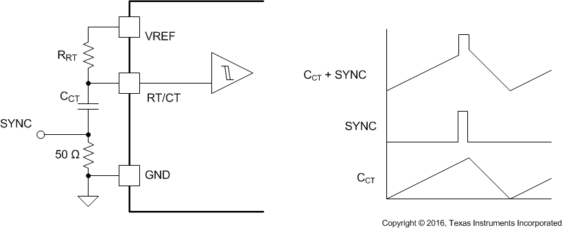
Synchronization is best achieved by forcing the timing capacitor voltage above the oscillator internal upper threshold. A small resistor is placed in series with CCT to GND. This resistor serves as the input for the sync pulse which raises the CCT voltage above the oscillator internal upper threshold. The PWM is allowed to run at the frequency set by RRT and CCT until the sync pulse appears. This scheme offers several advantages including having the local ramp available for slope compensation. The UCCx8C4x oscillator must be set to a lower frequency than the sync pulse stream, typically 20 percent with a 0.5V pulse applied across the resistor.
 Figure 7-5 Oscillator Synchronization Circuit