SLUS458I July 2000 – June 2024 UCC28C40 , UCC28C41 , UCC28C42 , UCC28C43 , UCC28C44 , UCC28C45 , UCC38C40 , UCC38C41 , UCC38C42 , UCC38C43 , UCC38C44 , UCC38C45
PRODUCTION DATA
- 1
- 1 Features
- 2 Applications
- 3 Description
- 4 Device Comparison Table
- 5 Pin Configuration and Functions
- 6 Specifications
-
7 Detailed Description
- 7.1 Overview
- 7.2 Functional Block Diagram
- 7.3
Feature Description
- 7.3.1 Detailed Pin Description
- 7.3.2 Undervoltage Lockout
- 7.3.3 ±1% Internal Reference Voltage
- 7.3.4 Current Sense and Overcurrent Limit
- 7.3.5 Reduced-Discharge Current Variation
- 7.3.6 Oscillator Synchronization
- 7.3.7 Soft-Start Timing
- 7.3.8 Enable and Disable
- 7.3.9 Slope Compensation
- 7.3.10 Voltage Mode
- 7.4 Device Functional Modes
-
8 Application and Implementation
- 8.1 Application Information
- 8.2
Typical Application
- 8.2.1 Design Requirements
- 8.2.2
Detailed Design Procedure
- 8.2.2.1 Input Bulk Capacitor and Minimum Bulk Voltage
- 8.2.2.2 Transformer Turns Ratio and Maximum Duty Cycle
- 8.2.2.3 Transformer Inductance and Peak Currents
- 8.2.2.4 Output Capacitor
- 8.2.2.5 Current Sensing Network
- 8.2.2.6 Gate Drive Resistor
- 8.2.2.7 VREF Capacitor
- 8.2.2.8 RT/CT
- 8.2.2.9 Start-Up Circuit
- 8.2.2.10 Voltage Feedback Compensation
- 8.2.3 Application Curves
- 8.3 Power Supply Recommendations
- 8.4 Layout
- 9 Device and Documentation Support
- 10Revision History
- 11Mechanical, Packaging, and Orderable Information
7.3.7 Soft-Start Timing
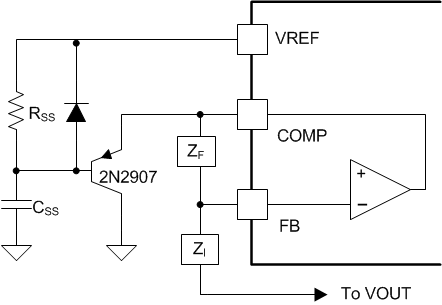
The soft-start timing is the technique to gradually power up the converter in a well-controlled fashion by slowly increasing the effective duty cycle starting at zero and gradually rising. Following start-up of the PWM, the error amplifier inverting input is low, commanding the error amplifier’s output to go high. The output stage of the amplifier can source 1mA typically, which is enough to drive most high impedance compensation networks, but not enough for driving large loads quickly. Soft-start timing is achieved by charging a fairly large value, >1µF, capacitor (CSS) connected to the error amplifier output through a PNP transistor as shown in Figure 7-6
 Figure 7-6 Soft-Start Implementation
The limited charging current of the amplifier into the capacitor translates into a dv/dt limitation on the error amplifier output. This directly corresponds to some maximum rate of change of primary current in a current mode controlled system as one of the PWM comparator inputs gradually rises. The values of RSS and CSS must be selected to bring the COMP pin up at a controlled rate, limiting the peak current supplied by the power stage. After the soft-start interval is complete, the capacitor continues to charge to VREF, effectively removing the PNP transistor from the circuit consideration. Soft-start timing offers a different, frequently preferred function in current mode controlled systems than it does in voltage mode control. In current mode, soft start controls the rising of the peak switch current. In voltage mode control, soft start gradually widens the duty cycle, regardless of the primary current or rate of ramp-up.
The purpose of resistor RSS and the diode is to remove the soft-start capacitor from the error amplifier path during normal operation, after the soft-start period completes and the capacitor charges fully. The optional diode in parallel with the resistor forces a soft-start period each time the PWM goes through UVLO condition that forces VREF to go low. Without the diode, the capacitor remains charged during a brief loss of supply or brown-out, and the device does not emable a soft-start function upon re-application of VDD.