SLUS495J August 2001 – December 2023 UCC29002 , UCC39002
PRODUCTION DATA
- 1
- 1Features
- 2Applications
- 3Description
- 4Pin Configuration and Functions
- 5Specifications
-
6Detailed Description
- 6.1 Overview
- 6.2 Functional Block Diagram
- 6.3
Feature Description
- 6.3.1 Differential Current-Sense Amplifier (CS+, CS−, CSO)
- 6.3.2 Load-Share Bus Driver Amplifier (CSO, LS)
- 6.3.3 Load-Share Bus Receiver Amplifier (LS)
- 6.3.4 Error Amplifier (EAO)
- 6.3.5 Adjust Amplifier Output (ADJ)
- 6.3.6 Enable Function (CS+, CS−)
- 6.3.7 Fault Protection on LS Bus
- 6.3.8 Start-Up and Adjust Logic
- 6.3.9 Bias Input and Bias_OK Circuit (VDD)
- 6.4 Device Functional Modes
- 7Application and Implementation
- 8Device and Documentation Support
- 9Revision History
- Mechanical, Packaging, and Orderable Information
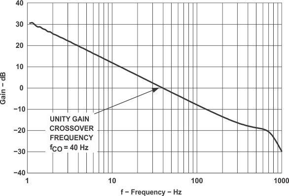
7.3.3 Application Curve
 Figure 7-6 Power Module Bode Plot