SLUS714E January 2007 – June 2019 TPS40077
PRODUCTION DATA.
- 1 Features
- 2 Applications
- 3 Description
- 4 Revision History
- 5 Pin Configuration and Functions
- 6 Specifications
-
7 Detailed Description
- 7.1 Overview
- 7.2 Functional Block Diagram
- 7.3
Feature Description
- 7.3.1 Minimum Pulse Duration
- 7.3.2 Slew Rate Limit On VDD
- 7.3.3 Setting The Switching Frequency (Programming The Clock Oscillator)
- 7.3.4 Loop Compensation
- 7.3.5 Shutdown and Sequencing
- 7.3.6 Boost and LVBP Bypass Capacitance
- 7.3.7 Internal Regulators
- 7.3.8 Power Dissipation
- 7.3.9 Boost Diode
- 7.3.10 Synchronous Rectifier Control
- 7.4 Programming
-
8 Application and Implementation
- 8.1 Application Information
- 8.2
Typical Applications
- 8.2.1
Buck Regulator 8-V to 16-V Input, 1.8-V Output at 10 A
- 8.2.1.1 Design Requirements
- 8.2.1.2
Detailed Design Procedure
- 8.2.1.2.1
Power Train Components
- 8.2.1.2.1.1 Output Inductor, LOUT
- 8.2.1.2.1.2 Output Capacitor, COUT, ELCO and MLCC
- 8.2.1.2.1.3 Input Capacitor, CIN ELCO and MLCC
- 8.2.1.2.1.4 Switching MOSFET, QSW
- 8.2.1.2.1.5 Rectifier MOSFET, QSR
- 8.2.1.2.1.6 Timing Resistor, RT
- 8.2.1.2.1.7 Feed-Forward and UVLO Resistor, RKFF
- 8.2.1.2.1.8 Soft-Start Capacitor, CSS
- 8.2.1.2.1.9 Short-Circuit Protection, RILIM and CILIM
- 8.2.1.2.1.10 Boost Voltage, CBOOST and DBOOST (Optional)
- 8.2.1.2.1.11 Closing the Feedback Loop, RZ1, RP1, RPZ2, RSET1, RSET2, CZ2, CP2, and CPZ1
- 8.2.1.2.1
Power Train Components
- 8.2.1.3 Application Curves
- 8.2.1
Buck Regulator 8-V to 16-V Input, 1.8-V Output at 10 A
- 8.3 Additional System Examples
- 9 Layout
- 10Device and Documentation Support
- 11Mechanical, Packaging, and Orderable Information
7.4.1 Programming The Ramp Generator Circuit and UVLO
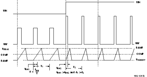
The ramp generator circuit provides the actual ramp used by the PWM comparator. The ramp generator provides voltage feed-forward control by varying the PWM ramp slope with line voltage, while maintaining a constant ramp magnitude. Varying the PWM ramp directly with line voltage provides excellent response to line variations, because the PWM is not required to wait for loop delays before changing the duty cycle. (See Figure 25).
The PWM ramp must reach approximately 1 V in amplitude during a clock cycle, or the PWM is not allowed to start. The PWM ramp time is programmed via a single resistor (RKFF) connected from KFF VDD. RKFF, VSTART, and RT are related by (approximately) Equation 10.

where
- RT and RKFF are in kΩ
- VUVLO(on) is in V
This yields typical numbers for the programmed start-up voltage. The minimum and maximum values may vary up to ±15% from this number. Figure 16 through Figure 18 show the typical relationship of VUVLO(on), VUVLO(off) and RKFF at three common frequencies.
The programmable UVLO circuit incorporates 20% hysteresis from the start voltage to the shutdown voltage. For example, if the start-up voltage is programmed to be 10 V, the controller starts when VDD reaches 10 V and shuts down when VDD falls below 8 V. The maximum duty cycle begins to decrease as the input voltage rises to twice the start-up voltage. Below this point, the maximum duty cycle is as specified in the Electrical Characteristics. Note that with this scheme, the theoretical maximum output voltage that the converter can produce is approximately two times the programmed start-up voltage. For design, set the programmed start-up voltage equal to or greater than the desired output voltage divided by maximum duty cycle (85% for frequencies 500 kHz and below). For example, a 5-V output converter should not have a programmed start-up voltage below 5.9 V. Figure 25 shows the theoretical maximum duty cycle (typical) for various programmed start-up voltages.
 Figure 25. Voltage Feed-Forward and PWM Duty Cycle Waveforms