SLUS720F February 2007 – June 2019 TPS40195
PRODUCTION DATA.
- 1 Features
- 2 Applications
- 3 Description
- 4 Revision History
- 5 Description (continued)
- 6 Pin Configuration and Functions
- 7 Specifications
- 8 Detailed Description
-
9 Application and Implementation
- 9.1 Application Information
- 9.2
Typical Applications
- 9.2.1
Typical Application 1
- 9.2.1.1 Design Requirements
- 9.2.1.2
Detailed Design Procedure
- 9.2.1.2.1 Output Inductor, LOUT
- 9.2.1.2.2 Output Capacitor, COUT
- 9.2.1.2.3 Input Capacitor, CIN
- 9.2.1.2.4 Switching MOSFET, QSW
- 9.2.1.2.5 Rectifier MOSFET, QSR
- 9.2.1.2.6
Component Selection for the TPS40195
- 9.2.1.2.6.1 Timing Resistor, RT
- 9.2.1.2.6.2 Setting UVLO
- 9.2.1.2.6.3 Setting the Soft-Start Time
- 9.2.1.2.6.4 Short-Circuit Protection, RILIM
- 9.2.1.2.6.5 Voltage Decoupling Capacitors, CBP, and CVDD
- 9.2.1.2.6.6 Boost Voltage, CBOOST and DBOOST (optional)
- 9.2.1.2.6.7 Closing the Feedback Loop RZ1, RP1, RPZ2, RSET1, RSET2, CZ2, CP2 AND CPZ1
- 9.2.1.2.7 Application Curve
- 9.2.2 Typical Application 2
- 9.2.3 Typical Application 3
- 9.2.1
Typical Application 1
- 10Layout
- 11Device and Documentation Support
- 12Mechanical, Packaging, and Orderable Information
8.3.6 Selecting the Short Circuit Threshold
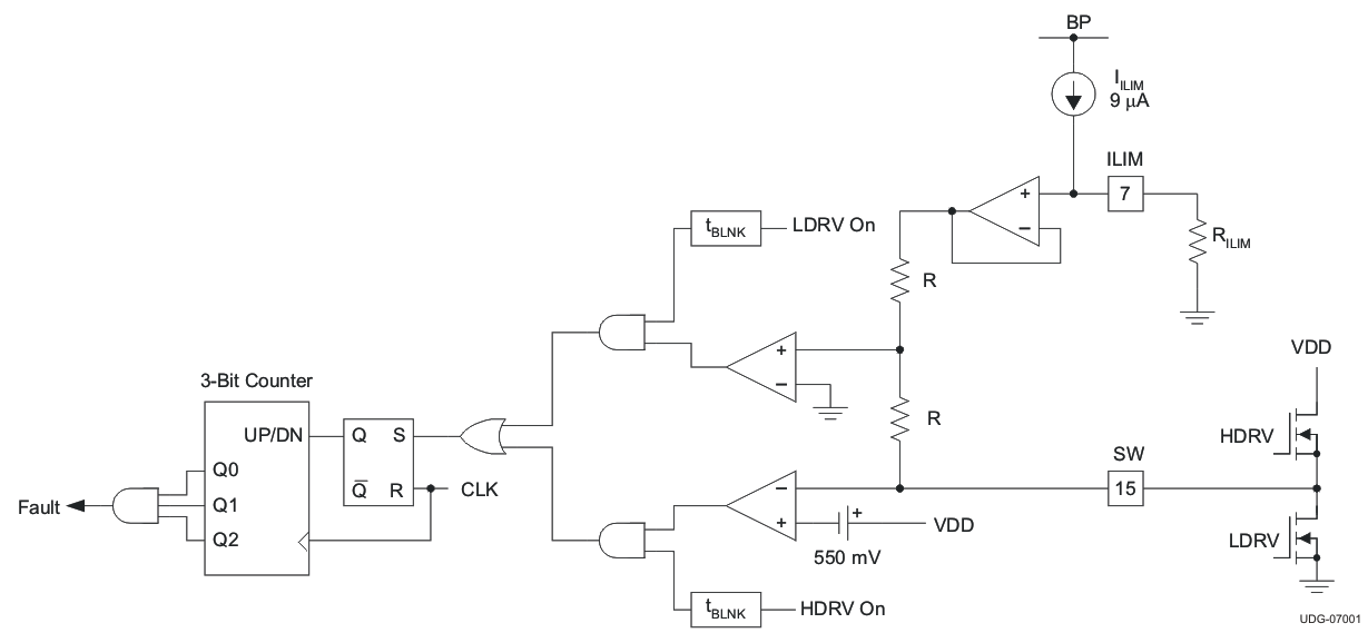
An over current is detected by sensing a voltage drop across the low-side FET when it is on, and across the high-side FET when it is on. If the voltage drop across either FET exceeds the short circuit threshold in any given switching cycle, a counter increments one count. If the voltage across the high-side FET was higher that the short circuit threshold, that FET is turned off early. If the voltage drop across either FET does not exceed the short circuit threshold during a cycle, the counter is decremented for that cycle. If the counter fills up (a count of 7) a fault condition is declared and the drivers turn off both MOSFETs. After a timeout of approximately 40 ms, the controller attempts to restart. If a short circuit remains present at the output, the current quickly ramps up to the short circuit threshold and another fault condition is declared and the process of waiting for the 40 ms and attempting to restart repeats.
The current limit threshold for the low-side FET is programmable by the user. To set the threshold a resistor is connected from the ILIM pin to GND. A current source inside the IC connected to the ILIM pin and this resistor set a voltage that is the threshold used for the overcurrent detection threshold. The low side threshold will increase as the low side on time decreases due to blanking time and comparator response time. See Figure 5 for changes in the threshold as the low-side FET conduction time decreases. Refer to Figure 21 for details on the functional equivalent schematic.
 Figure 21. Overcurrent

where
- IS.P. is the short circuit current
- IILIM is ILIM pin bias current, 9 μA (typical)
- RILIM is the resistance connected from ILIM to GND
- VILIMOFST is the offset voltage of the low side current sense comparator, ±20 mV
- RDS(on) is the channel resistance of the low-side MOSFET
The short circuit protection threshold for the high-side MOSFET is fixed at 550-mV typical, 400-mV minimum with a 4000 ppm/°C temperature coefficient to help compensate for changes in the high side FET channel resistance as temperature increases. This threshold is in place to provide a maximum current output in the case of a fault. The maximum amount of current that can be sourced from a converter can be found by Equation 7.

where
- IOUT(max) is the maximum current that the converter is specified to source
- VILIMH(min) is the short circuit threshold for the high-side MOSFET (400 mV)
- RDS(on)max is the maximum resistance of the high-side MOSFET
If the required current from the converter is greater than the calculated IOUT(max), a lower resistance high-side MOSFET must be chosen.
The length of time between restart attmepts after an output fault can be found from Equation 8.

where
- NDAC is the number of 1-V DAC ramp cycles from Table 2.
- fSW is the switching frequency in Hz