SLUS720F February   2007  – June 2019 TPS40195

PRODUCTION DATA.  

  1. Features
  2. Applications
  3. Description
    1.     Device Images
      1.      Simplified Application Diagram
  4. Revision History
  5. Description (continued)
  6. Pin Configuration and Functions
    1.     Pin Functions
  7. Specifications
    1. 7.1 Absolute Maximum Ratings
    2. 7.2 ESD Ratings
    3. 7.3 Recommended Operating Conditions
    4. 7.4 Electrical Characteristics
    5. 7.5 Dissipation Ratings
    6. 7.6 Typical Characteristics
  8. Detailed Description
    1. 8.1 Overview
    2. 8.2 Functional Block Diagram
    3. 8.3 Feature Description
      1. 8.3.1  Enable Functionality
      2. 8.3.2  Voltage Reference
      3. 8.3.3  Oscillator and Synchronization
      4. 8.3.4  Undervoltage Lockout (UVLO)
      5. 8.3.5  Soft Start
      6. 8.3.6  Selecting the Short Circuit Threshold
      7. 8.3.7  5-V Regulator
      8. 8.3.8  Prebias Start-up
      9. 8.3.9  Drivers
      10. 8.3.10 Power Good
      11. 8.3.11 Thermal Shutdown
  9. Application and Implementation
    1. 9.1 Application Information
    2. 9.2 Typical Applications
      1. 9.2.1 Typical Application 1
        1. 9.2.1.1 Design Requirements
        2. 9.2.1.2 Detailed Design Procedure
          1. 9.2.1.2.1 Output Inductor, LOUT
          2. 9.2.1.2.2 Output Capacitor, COUT
          3. 9.2.1.2.3 Input Capacitor, CIN
          4. 9.2.1.2.4 Switching MOSFET, QSW
          5. 9.2.1.2.5 Rectifier MOSFET, QSR
          6. 9.2.1.2.6 Component Selection for the TPS40195
            1. 9.2.1.2.6.1 Timing Resistor, RT
            2. 9.2.1.2.6.2 Setting UVLO
            3. 9.2.1.2.6.3 Setting the Soft-Start Time
            4. 9.2.1.2.6.4 Short-Circuit Protection, RILIM
            5. 9.2.1.2.6.5 Voltage Decoupling Capacitors, CBP, and CVDD
            6. 9.2.1.2.6.6 Boost Voltage, CBOOST and DBOOST (optional)
            7. 9.2.1.2.6.7 Closing the Feedback Loop RZ1, RP1, RPZ2, RSET1, RSET2, CZ2, CP2 AND CPZ1
          7. 9.2.1.2.7 Application Curve
      2. 9.2.2 Typical Application 2
        1. 9.2.2.1 Design Requirements
        2. 9.2.2.2 Detailed Design Procedure
        3. 9.2.2.3 Application Curves
      3. 9.2.3 Typical Application 3
        1. 9.2.3.1 Design Requirements
        2. 9.2.3.2 Detailed Design Procedure
        3. 9.2.3.3 Application Curves
  10. 10Layout
    1. 10.1 Layout Guidelines
    2. 10.2 Layout Examples
  11. 11Device and Documentation Support
    1. 11.1 Device Support
      1. 11.1.1 Third-Party Products Disclaimer
    2. 11.2 Device Support
      1. 11.2.1 Related Parts
    3. 11.3 Documentation Support
      1. 11.3.1 Related Documentation
    4. 11.4 Receiving Notification of Documentation Updates
    5. 11.5 Community Resources
    6. 11.6 Trademarks
    7. 11.7 Electrostatic Discharge Caution
    8. 11.8 Glossary
  12. 12Mechanical, Packaging, and Orderable Information

Typical Application 1

This section discusses basic buck converter design. Designers already familiar with the design of buck converters can skip to the next section Component Selection of this design example.
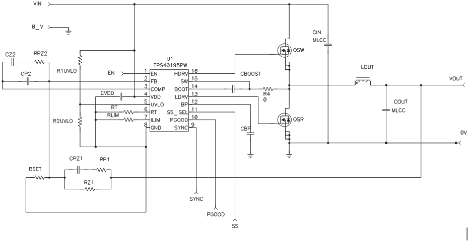
TPS40195 smdex3schem_lus720.gifFigure 22. TPS40195 Design Example Schematic