-
bq2438x Overvoltage and Overcurrent Protection IC and Li+ Charger Front-End Protection IC With LDO Mode
- 1 Features
- 2 Applications
- 3 Description
- 4 Revision History
- 5 Pin Configuration and Functions
- 6 Specifications
- 7 Detailed Description
- 8 Application and Implementation
- 9 Power Supply Recommendations
- 10Layout
- 11Device and Documentation Support
- 12Mechanical, Packaging, and Orderable Information
- IMPORTANT NOTICE
bq2438x Overvoltage and Overcurrent Protection IC and Li+ Charger Front-End Protection IC With LDO Mode
1 Features
- Input Overvoltage Protection
- Accurate Battery Overvoltage Protection
- Output Short-Circuit Protection
- Soft-Start to Prevent Inrush Currents
- Soft-Stop to Prevent Voltage Spikes
- Maximum Input Voltage of 30 V
- Supports up to 1.7-A Load Current
- Thermal Shutdown
- Enable Function
- Fault Status Indication
- Small 2 mm × 2 mm 8-Pin WSON Package
2 Applications
- Smart Phones, Mobile Phones
- PDAs
- MP3 Players
- Low-Power Handheld Devices
3 Description
The bq2438x family of devices are charger front-end integrated circuits (ICs) designed to provide protection to Li-ion batteries from failures of the charging circuit. The device continuously monitors the input voltage and battery voltage. The device operates like a linear regulator, maintaining a 5.5-V (bq24380) or 5-V (bq24381, bq24382) output with input voltages up to the Input overvoltage threshold. During input overvoltage conditions, the device immediately turns off the internal pass FET disconnecting the charging circuit from the damaging input source. Additionally, if the battery voltage rises to unsafe levels while charging, power is removed from the system. The device checks for short-circuit or overload conditions at its output when turning the pass FET on, and if it finds unsafe conditions, it switches off and then rechecks the conditions. Additionally, the device also monitors its die temperature and switches off if it exceeds 140°C.
When the device is controlled by a processor, the device provides status information about fault conditions to the host.
Device Information(1)
| PART NUMBER | PACKAGE | BODY SIZE (NOM) |
|---|---|---|
| bq24380 | WSON (8) | 2.00 mm × 2.00 mm |
| bq24381 | ||
| bq24382 |
- For all available packages, see the orderable addendum at the end of the data sheet.
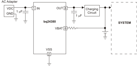
Simplified Schematic

4 Revision History
Changes from B Revision (March 2009) to C Revision
- Added ESD Ratings table, Thermal Information, Timing Requirements, Functional Block Diagram, Design Requirements, Application Curves, Power Supply Recommendations, Layout Example, Device and Documentation Support, and Mechanical, Packaging, and Orderable InformationGo
- Changed SON to WSON throughout the documentGo
- Changed From: "the bq2430x CE pin." To: "the bq2438x CE pin." in Selection of R(BAT)Go
- Moved Figures 1 through 8 from Typical Characteristics to Application Curves sectionGo
Changes from A Revision (May 2008) to B Revision
- Added device bq24382 to the datasheetGo
- Added the bq24382 option to IDD in the Electrical Characteristics.Go
- Added the bq24382 option to VO(REG) in theElectrical CharacteristicsGo
- Added the bq24382 option to VOVP in the Electrical CharacteristicsGo
- Added the bq24382 option to Vhys(OVP) in the Electrical CharacteristicsGo
Changes from * Revision (April 2008) to A Revision
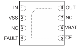
5 Pin Configuration and Functions

Pin Functions
| PIN | I/O | DESCRIPTION | |
|---|---|---|---|
| NAME | NO. | ||
| CE | 5 | I | Active-low chip enable input. Connect CE = HI to turn the input pass FET off. Connect CE = LOW to turn the internal pass FET on and connect the input to the charging circuitry. CE is Internally pulled down, approximately 200 kΩ. |
| FAULT | 4 | O | Open-drain device status output. FAULT is pulled to VSS internally when the input pass FET has been turned off due to input overvoltage or output short-circuit conditions, an overtemperature condition, or because the battery voltage is outside safe limits. FAULT is high impedance during normal operation. |
| IN | 1 | I | Input power, connected to external DC supply. Bypass IN to VSS with a ceramic capacitor (1 μF minimum) |
| NC | 3, 7 | Do not connect to any external circuits. These pins may have internal connections used for test purposes. | |
| OUT | 8 | O | Output terminal to the charging system. Bypass OUT to VSS with a ceramic capacitor (1 μF minimum) |
| VBAT | 6 | I | Battery voltage sense input. Connected to pack positive terminal through a 100-kΩ resistor. |
| VSS | 2 | – | Ground terminal. Connect to the thermal pad and to the ground rail of the circuit. |
| Thermal PAD | There is an internal electrical connection between the exposed thermal pad and the VSS pin of the device. The thermal pad must be connected to the same potential as the VSS pin on the printed-circuit board. Do not use the thermal pad as the primary ground input for the device. VSS pin must be connected to ground at all times. | ||