SLUS812D February 2008 – February 2020 TPS51200
PRODUCTION DATA.
- 1 Features
- 2 Applications
- 3 Description
- 4 Revision History
- 5 Pin Configuration and Functions
- 6 Specifications
-
7 Detailed Description
- 7.1 Overview
- 7.2 Functional Block Diagram
- 7.3
Feature Description
- 7.3.1 Sink and Source Regulator (VO Pin)
- 7.3.2 Reference Input (REFIN Pin)
- 7.3.3 Reference Output (REFOUT Pin)
- 7.3.4 Soft-Start Sequencing
- 7.3.5 Enable Control (EN Pin)
- 7.3.6 Powergood Function (PGOOD Pin)
- 7.3.7 Current Protection (VO Pin)
- 7.3.8 UVLO Protection (VIN Pin)
- 7.3.9 Thermal Shutdown
- 7.3.10 Tracking Start-up and Shutdown
- 7.3.11 Output Tolerance Consideration for VTT DIMM Applications
- 7.3.12 REFOUT (VREF) Consideration for DDR2 Applications
- 7.4 Device Functional Modes
- 8 Application and Implementation
- 9 Power Supply Recommendations
- 10Layout
- 11Device and Documentation Support
- 12Mechanical, Packaging, and Orderable Information
8.2.3 Application Curves
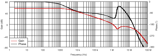
Figure 25 shows the bode plot simulation for this DDR3 design example of the TPS51200 device.
The unity-gain bandwidth is approximately 1 MHz and the phase margin is 52°. The 0-dB level is crossed, the gain peaks because of the ESL effect. However, the peaking maintains a level well below 0 dB.
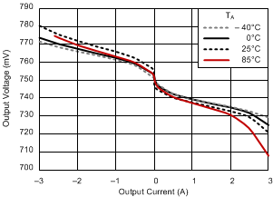
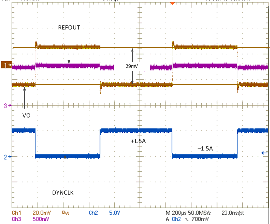
Figure 26 shows the load regulation and Figure 27 shows the transient response for a typical DDR3 configuration. When the regulator is subjected to ±1.5-A load step and release, the output voltage measurement shows no difference between the dc and ac conditions.

| VIN = 3.3 V | VVLDOIN = 1.5 V | VVO = 0.75 V | |
| IIO = 2 A | 3 × 10-μF capacitors | ESR = 2.5 mΩ | |
| ESL = 800 pH |

| VVIN = 3.3 V | DDR3 |
 Figure 27. Transient Waveform