SLUS846D September   2008  – August 2024 UCC25600

PRODUCTION DATA  

  1.   1
  2. Features
  3. Applications
  4. Description
  5. Revision History
  6. Pin Configuration and Functions
  7. Specifications
    1. 6.1 Absolute Maximum Ratings
    2. 6.2 ESD Ratings
    3. 6.3 Recommended Operating Conditions
    4. 6.4 Thermal Information
    5. 6.5 Electrical Characteristics
    6. 6.6 Typical Characteristics
  8. Detailed Description
    1. 7.1 Overview
    2. 7.2 Functional Block Diagram
    3. 7.3 Feature Description
      1. 7.3.1 Soft Start
      2. 7.3.2 Overcurrent Protection
      3. 7.3.3 Gate Driver
      4. 7.3.4 Overtemperature Protection
    4. 7.4 Device Functional Modes
      1. 7.4.1 Burst-Mode Operation
      2. 7.4.2 VCC
  9. Application and Implementation
    1. 8.1 Application Information
      1. 8.1.1 Principal of Operation
      2. 8.1.2 Adjustable Dead Time
      3. 8.1.3 Oscillator
    2. 8.2 Typical Application
      1. 8.2.1 Design Requirements
      2. 8.2.2 Detailed Design Procedure
      3. 8.2.3 Application Curves
  10. Power Supply Recommendations
  11. 10Layout
    1. 10.1 Layout Guidelines
    2. 10.2 Layout Example
  12. 11Device and Documentation Support
    1. 11.1 Support Resources
    2. 11.2 Trademarks
    3. 11.3 Electrostatic Discharge Caution
  13. 12Glossary
  14. 13Mechanical, Packaging, and Orderable Information

Typical Characteristics

At VCC = 12 V, RRT = 4.7 kΩ, RDT = 16.9 kΩ, VSS = 5 V, VOC = 0 V; all voltages are with respect to GND, TJ = TA = 25°C, unless otherwise noted.
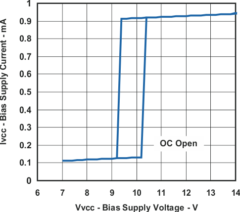
UCC25600 Bias Supply Current vs Bias Supply Voltage
Figure 6-1 Bias Supply Current vs Bias Supply Voltage
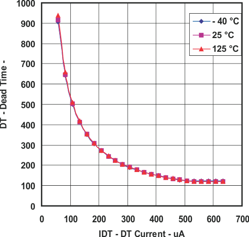
UCC25600 Dead Time vs DT Current
Figure 6-3 Dead Time vs DT Current
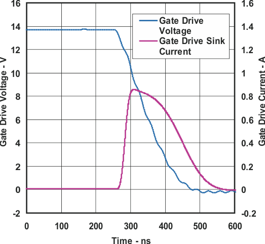
UCC25600 Gate Drive Falling, VCC = 15 V
Figure 6-5 Gate Drive Falling, VCC = 15 V
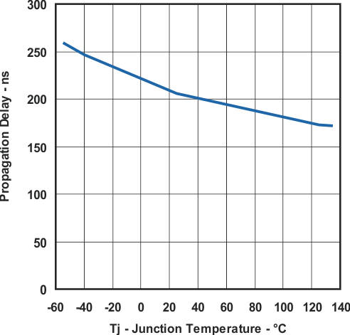
UCC25600 Overcurrent Propagation Delay vs Temperature
Figure 6-7 Overcurrent Propagation Delay vs Temperature
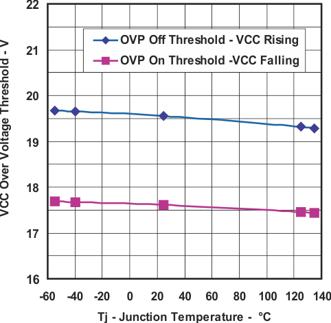
UCC25600 VCC Overvoltage Threshold vs Temperature
Figure 6-9 VCC Overvoltage Threshold vs Temperature
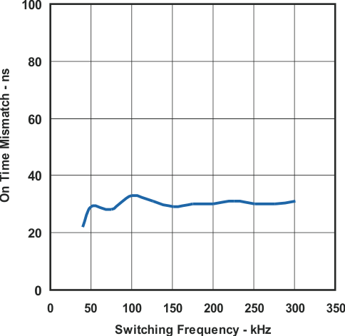
UCC25600 On-time Mismatch vs Switching Frequency
Figure 6-11 On-time Mismatch vs Switching Frequency
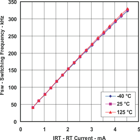
UCC25600 Switching Frequency vs RT Current
Figure 6-2 Switching Frequency vs RT Current
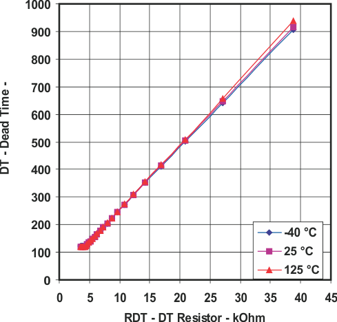
UCC25600 Dead Time vs DT Resistor
Figure 6-4 Dead Time vs DT Resistor
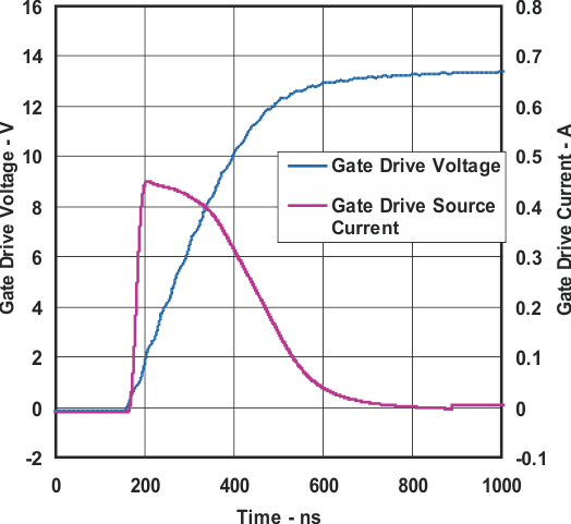
UCC25600 Gate Drive Rising, VCC = 15 V
Figure 6-6 Gate Drive Rising, VCC = 15 V
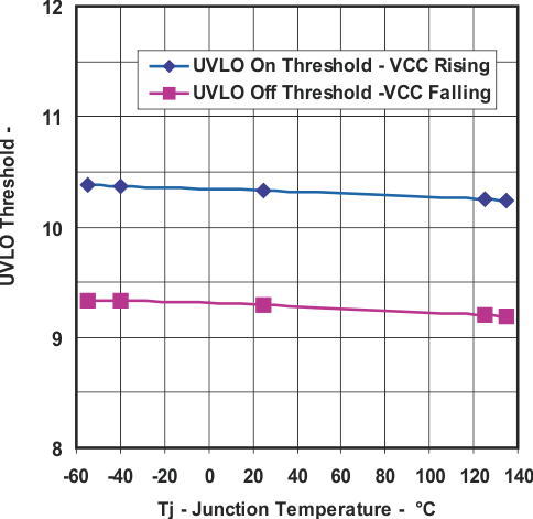
UCC25600 UVLO Threshold vs Temperature
Figure 6-8 UVLO Threshold vs Temperature
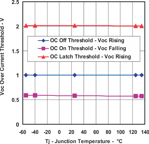
UCC25600 Overcurrent Threshold vs Temperature
Figure 6-10 Overcurrent Threshold vs Temperature