SLUS846D September 2008 – August 2024 UCC25600
PRODUCTION DATA
- 1
- 1 Features
- 2 Applications
- 3 Description
- 4 Revision History
- 5 Pin Configuration and Functions
- 6 Specifications
- 7 Detailed Description
- 8 Application and Implementation
- 9 Power Supply Recommendations
- 10Layout
- 11Device and Documentation Support
- 12Glossary
- 13Mechanical, Packaging, and Orderable Information
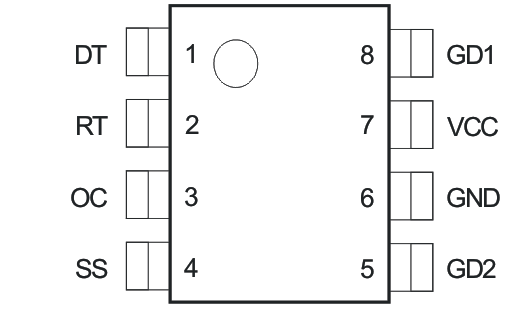
5 Pin Configuration and Functions
 Figure 5-1
D Package
8-Pin SOIC
Top View
Table 5-1 Pin Functions
| PIN | I/O | DESCRIPTION | |
|---|---|---|---|
| NAME | NO. | ||
| DT | 1 | I | This pin sets the dead time of high-side and low-side switch driving signals. Connect a resistor to ground. With internal 2.25-V voltage reference, the current flowing through the resistor sets the dead time. To prevent shoot through when this pin is accidentally shorted to ground, the minimum dead time is set to 120 ns. Any dead time setting less than 120 ns will automatically have 120-ns dead time. |
| GD1 | 8 | O | High-side and low-side switch gate driver. Connect gate driver transformer primary side to these two pins to drive the half-bridge. |
| GD2 | 5 | ||
| GND | 6 | — | Ground |
| OC | 3 | I | Overcurrent protection pin. When the voltage on this pin is above 1 V, gate driver signals are actively pulled low. After the voltage falls below 0.6 V, the gate driver signal recovers with soft-start. When OC pin voltage is above 2 V, the device is latched off. Bringing VCC below the UVLO level resets the overcurrent latch to off. |
| RT | 2 | I | The current flowing out of this pin sets the frequency of the gate driver signals. Connect the opto-coupler collector to this pin to control the switching frequency for regulation purposes. Parallel a resistor to ground to set the minimum current flowing out of the pin and set the minimum switching frequency. To set the maximum switching frequency limiting, simply series a resistor with the opto-coupler transistor. This resistor sets the maximum current flowing out of the pin and limits the maximum switching frequency. |
| SS | 4 | I | Soft-start pin. This pin sets the soft-start time of the system. Connect a capacitor to ground. Pulling this pin below 1 V will disable the device to allow easy ON/OFF control. The soft-start function is enabled after all fault conditions, including bias supply OV, UVLO, overcurrent protection, and overtemperature protection. |
| VCC | 7 | — | Bias Supply. Connect this pin to a power supply less than 20 V. Parallel a 1-μF capacitor to ground to filter out noise. |