TPS54233 2A, 28V Input, Step Down DC/DC Converter With Eco-mode™
1 Features
- 3.5 V to 28 V Input Voltage Range
- Adjustable Output Voltage Down to 0.8 V
- Integrated 80 mΩ High Side MOSFET Supports up to 2A Continuous Output Current
- High Efficiency at Light Loads with a Pulse Skipping Eco-mode™
- Fixed 300 kHz Switching Frequency
- Typical 1 μA Shutdown Quiescent Current
- Adjustable Slow Start Limits Inrush Currents
- Programmable UVLO Threshold
- Overvoltage Transient Protection
- Cycle by Cycle Current Limit, Frequency Fold Back and Thermal Shutdown Protection
- Available in Easy-to-Use SOIC8 Package
- Supported by WEBENCH® Software Tool (www.TI.com/WEBENCH)
2 Applications
- Consumer Applications such as Set-Top Boxes, CPE Equipment, LCD Displays, Peripherals, and Battery Chargers
- Industrial and Car Audio Power Supplies
- 5V, 12V and 24V Distributed Power Systems
3 Description
The TPS54233 is a 28 V, 2 A non-synchronous buck converter that integrates a low RDS(on) high side MOSFET. To increase efficiency at light loads, a pulse skipping Eco-mode™ feature is automatically activated. Furthermore, the 1 μA shutdown supply current allows the device to be used in battery powered applications. Current mode control with internal slope compensation simplifies the external compensation calculations and reduces component count while allowing the use of ceramic output capacitors. A resistor divider programs the Hysteresis of the input under-voltage lockout. An overvoltage transient protection circuit limits voltage overshoots during startup and transient conditions. A cycle by cycle current limit scheme, frequency fold back and thermal shutdown protect the device and the load in the event of an overload condition. The TPS54233 is available in an 8-pin SOIC package that has been internally optimized to improve thermal performance.
Device Information(1)
| PART NUMBER | PACKAGE | BODY SIZE (NOM) |
|---|---|---|
| TPS54233 | SOIC (8) | 4.90 mm x 3.90 mm |
- For all available packages, see the orderable addendum at the end of the data sheet.
5 Revision History
Changes from B Revision (February 2011) to C Revision
- Added ESD Rating table, Thermal Information table, Feature Description section, Device Functional Modes, Application and Implementation section, Power Supply Recommendations section, Device and Documentation Support section, and Mechanical, Packaging sections. Go
- Deleted Features Item: For SWIFT™ Documentation, See the TI Website at www.ti.com/swiftGo
- Changed Features item: Supported by SwitcherPro™ To: Supported by WEBENCH®Go
- Changed RO1 To: R5, RO2 To R6, C1 To C6, and C2 To C7 in the Simplified SchematicGo
- Changed SwitcherPro™ Software tool To: WEBENCH Software tool in the Current Mode Compensation Design sectionGo
- Changed RO1 To: R5, RO2 To R6, C1 To C6, and C2 To C7 in the Table 1Go
- Changed the Output Voltage Set Point section. Updated the paragraph following Equation 5.Go
Changes from A Revision (March 2010) to B Revision
Changes from * Revision (October 2008) to A Revision
- Changed the Absolute Maximum Ratings table, Input Voltage - EN pin max value From: 5V to 6VGo
- Added A table to the Description - with text "For additional design needs, see.."Go
6 Pin Configuration and Functions

Pin Functions
| PIN | DESCRIPTION | |
|---|---|---|
| NAME | NO. | |
| BOOT | 1 | A 0.1 μF bootstrap capacitor is required between BOOT and PH. If the voltage on this capacitor falls below the minimum requirement, the high-side MOSFET is forced to switch off until the capacitor is refreshed. |
| VIN | 2 | Input supply voltage, 3.5 V to 28 V. |
| EN | 3 | Enable pin. Pull below 1.25V to disable. Float to enable. Programming the input undervoltage lockout with two resistors is recommended. |
| SS | 4 | Slow start pin. An external capacitor connected to this pin sets the output rise time. |
| VSENSE | 5 | Inverting node of the gm error amplifier. |
| COMP | 6 | Error amplifier output, and input to the PWM comparator. Connect frequency compensation components to this pin. |
| GND | 7 | Ground. |
| PH | 8 | The source of the internal high-side power MOSFET. |
7 Specifications
7.1 Absolute Maximum Ratings(1)
over operating free-air temperature range (unless otherwise noted)7.2 ESD Ratings
| VALUE | UNIT | |||
|---|---|---|---|---|
| V(ESD) | Electrostatic discharge | Human-body model (HBM), per ANSI/ESDA/JEDEC JS-001(1) | ±2000 | V |
| Charged-device model (CDM), per JEDEC specification JESD22-C101(2) | ±500 | |||
7.3 Recommended Operating Conditions
over operating free-air temperature range (unless otherwise noted)| MIN | TYP | MAX | UNIT | |
|---|---|---|---|---|
| Operating Input Voltage on (VIN pin) | 3.5 | 28 | V | |
| Operating junction temperature, TJ | –40 | 150 | °C |
7.4 Thermal Information
| THERMAL METRIC(1) | D | UNIT | |
|---|---|---|---|
| 8 PINS | |||
| RθJA | Junction-to-ambient thermal resistance | 116.7 | °C/W |
| RθJC(top) | Junction-to-case (top) thermal resistance | 62.4 | |
| RθJB | Junction-to-board thermal resistance | 57.0 | |
| ψJT | Junction-to-top characterization parameter | 14.5 | |
| ψJB | Junction-to-board characterization parameter | 56.5 | |
| RθJC(bot) | Junction-to-case (bottom) thermal resistance | N/A | |
7.5 Electrical Characteristics
TJ = –40°C to 150°C, VIN = 3.5V to 28V (unless otherwise noted)| PARAMETER | TEST CONDITIONS | MIN | TYP | MAX | UNIT |
|---|---|---|---|---|---|
| SUPPLY VOLTAGE (VIN PIN) | |||||
| Internal undervoltage lockout threshold | Rising and Falling | 3.5 | V | ||
| Shutdown supply current | EN = 0V, VIN = 12V, –40°C to 85°C | 1 | 4 | μA | |
| Operating – non switching supply current | VSENSE = 0.85 V | 75 | 110 | μA | |
| ENABLE AND UVLO (EN PIN) | |||||
| Enable threshold | Rising and Falling | 1.25 | 1.35 | V | |
| Input current | Enable threshold – 50 mV | -1 | μA | ||
| Input current | Enable threshold + 50 mV | -4 | μA | ||
| VOLTAGE REFERENCE | |||||
| Voltage reference | 0.772 | 0.8 | 0.828 | V | |
| HIGH-SIDE MOSFET | |||||
| On resistance | BOOT-PH = 3 V, VIN = 3.5 V | 115 | 200 | mΩ | |
| BOOT-PH = 6 V, VIN = 12 V | 80 | 150 | |||
| ERROR AMPLIFIER | |||||
| Error amplifier transconductance (gm) | –2 μA < I(COMP) < 2 μA, V(COMP) = 1 V | 92 | μmhos | ||
| Error amplifier DC gain(1) | VSENSE = 0.8 V | 800 | V/V | ||
| Error amplifier unity gain bandwidth(1) | 5 pF capacitance from COMP to GND pins | 2.7 | MHz | ||
| Error amplifier source/sink current | V(COMP) = 1 V, 100 mV overdrive | ±7 | μA | ||
| Switch current to COMP transconductance | VIN = 12 V | 9 | A/V | ||
| PULSE SKIPPING Eco-mode™ | |||||
| Pulse skipping Eco-mode™ switch current threshold | 100 | mA | |||
| CURRENT LIMIT | |||||
| Current limit threshold | VIN = 12 V | 2.3 | 3.5 | A | |
| THERMAL SHUTDOWN | |||||
| Thermal Shutdown | 165 | °C | |||
| SLOW START (SS PIN) | |||||
| Charge current | V(SS) = 0.4 V | 2 | μA | ||
| SS to VSENSE matching | V(SS) = 0.4 V | 10 | mV | ||
7.6 Switching Characteristics
TJ = –40°C to 150°C, VIN = 3.5 to 28 V (unless otherwise noted)| PARAMETER | TEST CONDITIONS | MIN | TYP | MAX | UNIT | |
|---|---|---|---|---|---|---|
| SWITCHING FREQUENCY | ||||||
| Device switching frequency | VIN = 12 V | 210 | 300 | 390 | kHz | |
| Minimum controllable on time | VIN = 12 V, 25°C | 105 | 130 | ns | ||
| Maximum controllable duty ratio(1) | BOOT-PH = 6 V | 90% | 93% | |||
7.7 Typical Characteristics
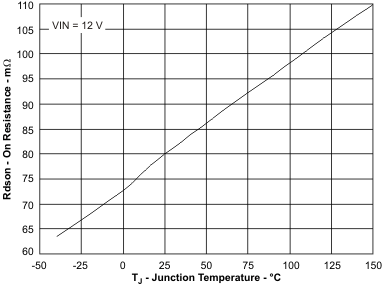 Figure 1. On Resistance vs Junction Temperature
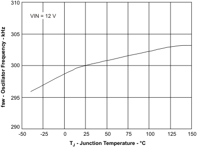 Figure 3. Switching Frequency vs Junction Temperature
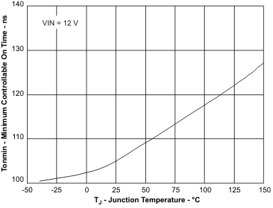 Figure 5. Minimum Controllable On Time vs
 Junction Temperature
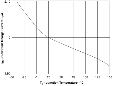 Figure 7. SS Charge Current vs Junction Temperature
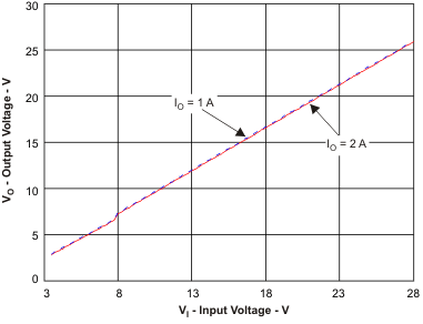 Figure 9. Typical Maximum Output Voltage vs
 Input Voltage
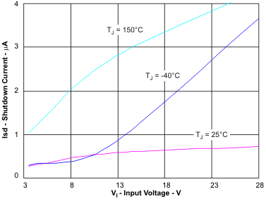 Figure 2. Shutdown Quiescent Current vs Input Voltage
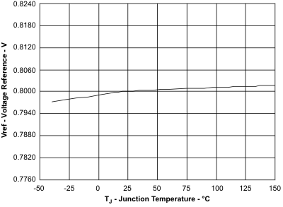 Figure 4. Voltage Reference vs Junction Temperature
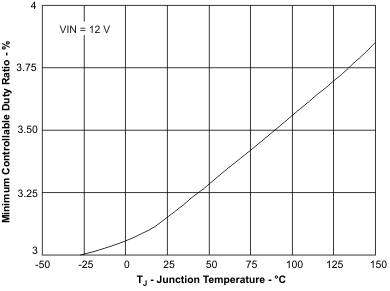 Figure 6. Minimum Controllable Duty Ratio vs
 Junction Temperature
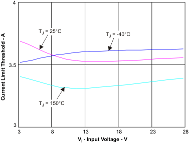 Figure 8. Current Limit Threshold vs Input Voltage
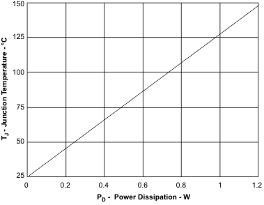 Figure 10. Maximum Power Dissipation vs
 Junction Temperature
8 Detailed Description
8.1 Overview
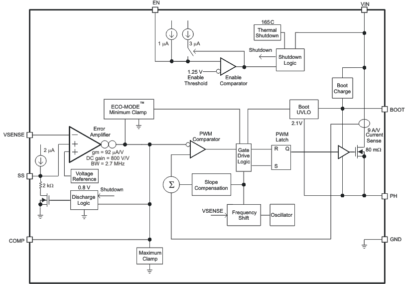
The TPS54233 is a 28 V, 2 A, step-down (buck) converter with an integrated high-side n-channel MOSFET. To improve performance during line and load transients, the device implements a constant frequency, current mode control which reduces output capacitance and simplifies external frequency compensation design. The TPS54233 has a pre-set switching frequency of 300 kHz.
The TPS54233 needs a minimum input voltage of 3.5 V to operate normally. The EN pin has an internal pull-up current source that can be used to adjust the input voltage under-voltage lockout (UVLO) with two external resistors. In addition, the pull-up current provides a default condition when the EN pin is floating for the device to operate. The operating current is 75 μA typically when not switching and under no load. When the device is disabled, the supply current is 1 μA typically.
The integrated 80 mΩ high-side MOSFET allows for high efficiency power supply designs with continuous output currents up to 2 A.
The TPS54233 reduces the external component count by integrating the boot recharge diode. The bias voltage for the integrated high-side MOSFET is supplied by an external capacitor on the BOOT to PH pin. The boot capacitor voltage is monitored by an UVLO circuit and will turn the high-side MOSFET off when the voltage falls below a preset threshold of 2.1 V typically. The output voltage can be stepped down to as low as the reference voltage.
By adding an external capacitor, the slow start time of the TPS54233 can be adjustable which enables flexible output filter selection.
To improve the efficiency at light load conditions, the TPS54233 enters a special pulse skipping Eco-modeTM when the peak inductor current drops below 100 mA typically.
The frequency foldback reduces the switching frequency during startup and over current conditions to help control the inductor current. The thermal shut down gives the additional protection under fault conditions.
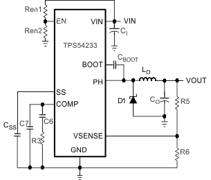
Functional Block Diagram
8.2 Feature Description
8.2.1 Fixed Frequency PWM Control
The TPS54233 uses a fixed frequency, peak current mode control. The internal switching frequency of the TPS54233 is fixed at 300kHz.
8.2.2 Voltage Reference (Vref)
The voltage reference system produces a ±2% initial accuracy voltage reference (±3.5% over temperature) by scaling the output of a temperature stable bandgap circuit. The typical voltage reference is designed at 0.8V.
8.2.3 Bootstrap Voltage (BOOT)
The TPS54233 has an integrated boot regulator and requires a 0.1 μF ceramic capacitor between the BOOT and PH pin to provide the gate drive voltage for the high-side MOSFET. A ceramic capacitor with an X7R or X5R grade dielectric is recommended because of the stable characteristics over temperature and voltage. To improve drop out, the TPS54233 is designed to operate at 100% duty cycle as long as the BOOT to PH pin voltage is greater than 2.1V typically.
8.2.4 Enable and Adjustable Input Under-Voltage Lockout (VIN UVLO)
The EN pin has an internal pull-up current source that provides the default condition of the TPS54233 operating when the EN pin floats.
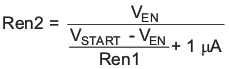
The TPS54233 is disabled when the VIN pin voltage falls below internal VIN UVLO threshold. It is recommended to use an external VIN UVLO to add Hysteresis unless VIN is greater than (VOUT + 2V). To adjust the VIN UVLO with Hysteresis, use the external circuitry connected to the EN pin as shown in Figure 11. Once the EN pin voltage exceeds 1.25V , an additional 3 μA of hysteresis is added. Use Equation 1 and Equation 2 to calculate the resistor values needed for the desired VIN UVLO threshold voltages. The VSTART is the input start threshold voltage, the VSTOP is the input stop threshold voltage and the VEN is the enable threshold voltage of 1.25 V. The VSTOP should always be greater than 3.5 V.
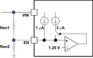 Figure 11. Adjustable Input Undervoltage Lockout

8.2.5 Programmable Slow Start Using SS PIN
It is recommended to program the slow start time externally because no slow start time is implemented internally. The TPS54233 effectively uses the lower voltage of the internal voltage reference or the SS pin voltage as the power supply’s reference voltage fed into the error amplifier and will regulate the output accordingly. A capacitor (CSS) on the SS pin to ground implements a slow start time. The TPS54233 has an internal pull-up current source of 2 μA that charges the external slow start capacitor. The equation for the slow start time (10% to 90%) is shown in Equation 3 . The Vref is 0.8 V and the ISS current is 2 μA.

The slow start time should be set between 1ms to 10ms to ensure good start-up behavior. The slow start capacitor should be no more than 27 nF.
If during normal operation, the input voltage drops below the VIN UVLO threshold, or the EN pin is pulled below 1.25 V, or a thermal shutdown event occurs, the TPS54233 stops switching.
8.2.6 Error Amplifier
The TPS54233 has a transconductance amplifier for the error amplifier. The error amplifier compares the VSENSE voltage to the internal effective voltage reference presented at the input of the error amplifier. The transconductance of the error amplifier is 92 μA/V during normal operation. Frequency compensation components are connected between the COMP pin and ground.
8.2.7 Slope Compensation
To prevent the sub-harmonic oscillations when operating the device at duty cycles greater than 50%, the TPS54233 adds a built-in slope compensation which is a compensating ramp to the switch current signal.
8.2.8 Current Mode Compensation Design
To simplify design efforts using the TPS54233, the typical designs for common applications are listed in Table 1. For designs using ceramic output capacitors, proper derating of ceramic output capacitance is recommended when doing the stability analysis. This is because the actual ceramic capacitance drops considerably from the nominal value when the applied voltage increases. See the Detailed Design Procedure section for the detailed guidelines or use the WEBENCH Software tool (www.TI.com/WEBENCH).
Table 1. Typical Designs (Refer to Section 4: Simplified Schematic
| VIN (V) |
VOUT
(V) |
Fsw
(kHz) |
LO
(μH) |
CO
|
R5 (kΩ) |
R6 (kΩ) |
C7 (pF) |
C6 (pF) |
R3 (kΩ) |
|---|---|---|---|---|---|---|---|---|---|
| 12 | 5 | 300 | 22 | Ceramic 47 μF | 10 | 1.91 | 68 | 1800 | 21 |
| 12 | 3.3 | 300 | 15 | Ceramic 47μF | 10.2 | 3.24 | 47 | 4700 | 21 |
| 12 | 1.8 | 300 | 10 | Ceramic 100 μF x 2 | 10 | 8.06 | 100 | 4700 | 21 |
| 12 | 0.9 | 300 | 6.8 | Ceramic 100 μFx2 | 10 | 80.6 | 100 | 4700 | 21 |
| 12 | 5 | 300 | 22 | Aluminum 330 μF/160 mΩ | 10 | 1.91 | 56 | 220 | 40.2 |
| 12 | 3.3 | 300 | 15 | Aluminum 470 μF/160 mΩ | 10.2 | 3.24 | 220 | 220 | 30.9 |
| 12 | 1.8 | 300 | 10 | SP 220 μF/12 mΩ | 10 | 8.06 | 100 | 4700 | 40.2 |
| 12 | 0.9 | 300 | 6.8 | SP 220 μF/12 mΩ | 10 | 80.6 | 100 | 1800 | 21 |
8.2.9 Overcurrent Protection and Frequency Shift
The TPS54233 implements current mode control that uses the COMP pin voltage to turn off the high-side MOSFET on a cycle by cycle basis. Every cycle the switch current and the COMP pin voltage are compared; when the peak inductor current intersects the COMP pin voltage, the high-side switch is turned off. During overcurrent conditions that pull the output voltage low, the error amplifier responds by driving the COMP pin high, causing the switch current to increase. The COMP pin has a maximum clamp internally, which limit the output current.
The TPS54233 provides robust protection during short circuits. There is potential for overcurrent runaway in the output inductor during a short circuit at the output. The TPS54233 solves this issue by increasing the off time during short circuit conditions by lowering the switching frequency. The switching frequency is divided by 8, 4, 2, and 1 as the voltage ramps from 0 V to 0.8 V on VSENSE pin. The relationship between the switching frequency and the VSENSE pin voltage is shown in Table 2.
Table 2. Switching Frequency Conditions
| SWITCHING FREQUENCY | VSENSE PIN VOLTAGE |
|---|---|
| 300 kHz | VSENSE ≥ 0.6 V |
| 300 kHz / 2 | 0.6 V > VSENSE ≥ 0.4 V |
| 300 kHz / 4 | 0.4 V > VSENSE ≥ 0.2 V |
| 300 kHz / 8 | 0.2 V > VSENSE |
8.2.10 Overvoltage Transient Protection
The TPS54233 incorporates an overvoltage transient protection (OVTP) circuit to minimize output voltage overshoot when recovering from output fault conditions or strong unload transients. The OVTP circuit includes an overvoltage comparator to compare the VSENSE pin voltage and internal thresholds. When the VSENSE pin voltage goes above 109% × Vref, the high-side MOSFET will be forced off. When the VSENSE pin voltage falls below 107% × Vref, the high-side MOSFET will be enabled again.
8.2.11 Thermal Shutdown
The device implements an internal thermal shutdown to protect itself if the junction temperature exceeds 165°C. The thermal shutdown forces the device to stop switching when the junction temperature exceeds the thermal trip threshold. Once the die temperature decreases below 165°C, the device reinitiates the power up sequence.
8.3 Device Functional Modes
8.3.1 Eco-modeTM
The TPS54233 is designed to operate in pulse skipping Eco-modeTM at light load currents to boost light load efficiency. When the peak inductor current is lower than 100 mA typically, the COMP pin voltage falls to 0.5V typically and the device enters Eco-mode™. When the device is in Eco-mode™, the COMP pin voltage is clamped at 0.5V internally which prevents the high side integrated MOSFET from switching. The peak inductor current must rise above 100mA for the COMP pin voltage to rise above 0.5V and exit Eco-mode™. Since the integrated current comparator catches the peak inductor current only, the average load current entering Eco-mode™ varies with the applications and external output filters.