SLUSA13E February   2010  – November 2023 UCC27321-Q1 , UCC27322-Q1

PRODUCTION DATA  

  1.   1
  2. Features
  3. Applications
  4. Description
  5. Description (continued)
  6. Related Products
  7. Pin Configuration and Functions
  8. Specifications
    1. 7.1 Absolute Maximum Ratings
    2. 7.2 ESD Ratings
    3. 7.3 Recommended Operating Conditions
    4. 7.4 Thermal Information
    5. 7.5 Electrical Characteristics
    6. 7.6 Switching Characteristics
    7. 7.7 Typical Characteristics
  9. Detailed Description
    1. 8.1 Overview
    2. 8.2 Functional Block Diagram
    3. 8.3 Feature Description
      1. 8.3.1 Input Stage
      2. 8.3.2 Output Stage
      3. 8.3.3 Source and Sink Capabilities During Miller Plateau
      4. 8.3.4 VDD
      5. 8.3.5 Drive Current and Power Requirements
      6. 8.3.6 Enable
    4. 8.4 Device Functional Modes
  10. Application and Implementation
    1. 9.1 Application Information
    2. 9.2 Typical Application
      1. 9.2.1 Design Requirements
      2. 9.2.2 Detailed Design Procedure
        1. 9.2.2.1 Input-to-Output Configuration
        2. 9.2.2.2 Input Threshold Type
        3. 9.2.2.3 VDD Bias Supply Voltage
        4. 9.2.2.4 Peak Source and Sink Currents
        5. 9.2.2.5 Enable and Disable Function
        6. 9.2.2.6 Propagation Delay
      3. 9.2.3 Application Curves
  11. 10Power Supply Recommendations
    1.     40
  12. 11Layout
    1. 11.1 Layout Guidelines
    2. 11.2 Layout Example
    3. 11.3 Thermal Considerations
    4. 11.4 Power Dissipation
  13. 12Device and Documentation Support
    1. 12.1 Device Support
      1. 12.1.1 Third-Party Products Disclaimer
    2. 12.2 Documentation Support
      1. 12.2.1 Related Documentation
    3. 12.3 Receiving Notification of Documentation Updates
    4. 12.4 Support Resources
    5. 12.5 Trademarks
    6. 12.6 Electrostatic Discharge Caution
    7. 12.7 Glossary
  14. 13Revision History
  15. 14Mechanical, Packaging, and Orderable Information

Switching Characteristics

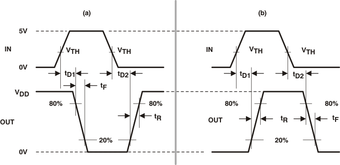
VDD = 4.5 V to 15 V, TJ = TA = –40°C to 125°C (unless otherwise noted) (see Figure 7-1)
PARAMETERTEST CONDITIONSMINTYPMAXUNIT
tRRise time (OUT)CLOAD = 10 nF2075ns
tFFall time (OUT)CLOAD = 10 nF2035ns
tD1Delay time, IN rising (IN to OUT)CLOAD = 10 nF2575ns
tD2Delay time, IN falling (IN to OUT)CLOAD = 10 nF3575ns
GUID-36D50241-AFBD-442E-93D4-6009B72D2614-low.gif
The 20% and 80% thresholds depict the dynamics of the bipolar output devices that dominate the power MOSFET transition through the Miller regions of operation.
Figure 7-1 Switching Waveforms for Inverting Driver (a) and Noninverting Driver (b)
GUID-C14DDA50-A659-4FF5-8FB2-EB3DD9B3E94D-low.gif
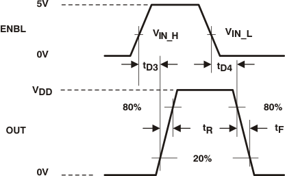
The 20% and 80% thresholds depict the dynamics of the bipolar output devices that dominate the power MOSFET transition through the Miller regions of operation.
Figure 7-2 Switching Waveforms for Enable to Output