SLUSAD2C November 2010 – April 2015 BQ24170 , BQ24172
PRODUCTION DATA.
- 1 Features
- 2 Applications
- 3 Description
- 4 Revision History
- 5 Description (continued)
- 6 Device Comparison Table
- 7 Pin Configuration and Functions
- 8 Specifications
-
9 Detailed Description
- 9.1 Overview
- 9.2 Functional Block Diagram
- 9.3
Feature Description
- 9.3.1 Battery Voltage Regulation
- 9.3.2 Battery Current Regulation
- 9.3.3 Battery Precharge Current Regulation
- 9.3.4 Input Current Regulation
- 9.3.5 Charge Termination, Recharge, and Safety Timers
- 9.3.6 Power Up
- 9.3.7 Input Undervoltage Lockout (UVLO)
- 9.3.8 Input Overvoltage/Undervoltage Protection
- 9.3.9 Enable and Disable Charging
- 9.3.10 System Power Selector
- 9.3.11 Converter Operation
- 9.3.12 Automatic Internal Soft-Start Charger Current
- 9.3.13 Charge Overcurrent Protection
- 9.3.14 Charge Undercurrent Protection
- 9.3.15 Battery Detection
- 9.3.16 Battery Short Protection
- 9.3.17 Battery Overvoltage Protection
- 9.3.18 Temperature Qualification
- 9.3.19 MOSFET Short Circuit and Inductor Short Circuit Protection
- 9.3.20 Thermal Regulation and Shutdown Protection
- 9.3.21 Timer Fault Recovery
- 9.3.22 Inductor, Capacitor, and Sense Resistor Selection Guidelines
- 9.3.23 Charge Status Outputs
- 9.4 Device Functional Modes
- 10Application and Implementation
- 11Power Supply Recommendations
- 12Layout
- 13Device and Documentation Support
- 14Mechanical, Packaging, and Orderable Information
8 Specifications
8.1 Absolute Maximum Ratings
over operating free-air temperature range (unless otherwise noted) (1)(2)(1) Stresses beyond those listed under Absolute Maximum Ratings may cause permanent damage to the device. These are stress ratings only, and functional operation of the device at these or any other conditions beyond those indicated under Recommended Operating Conditions is not implied. Exposure to absolute-maximum-rated conditions for extended periods may affect device reliability.
(2) All voltages are with respect to GND if not specified. Currents are positive into, negative out of the specified terminal. Consult packaging section of the data book for thermal limitations and considerations of packages.
8.2 ESD Ratings
| VALUE | UNIT | |||
|---|---|---|---|---|
| V(ESD) | Electrostatic discharge | Human body model (HBM), per ANSI/ESDA/JEDEC JS-001(1) | 1000 | V |
| Charged device model (CDM), per JEDEC specification JESD22-C101(2) | 250 | |||
(1) JEDEC document JEP155 states that 500-V HBM allows safe manufacturing with a standard ESD control process.
(2) JEDEC document JEP157 states that 250-V CDM allows safe manufacturing with a standard ESD control process.
8.3 Recommended Operating Conditions
8.4 Thermal Information
| THERMAL METRIC(1) | bq2417x | UNIT | |
|---|---|---|---|
| RGY [VQFN] | |||
| 24 PINS | |||
| RθJA | Junction-to-ambient thermal resistance | 35.7 | °C/W |
| ψJT | Junction-to-top characterization parameter | 0.4 | |
| ψJB | Junction-to-board characterization parameter | 31.2 | |
(1) For more information about traditional and new thermal metrics, see the IC Package Thermal Metrics application report, SPRA953.
8.5 Electrical Characteristics
4.5 V ≤ V(PVCC, AVCC) ≤ 17 V, –40°C < TJ + 125°C, typical values are at TA = 25°C, with respect to AGND (unless otherwise noted)| PARAMETER | TEST CONDITIONS | MIN | TYP | MAX | UNIT | |
|---|---|---|---|---|---|---|
| OPERATING CONDITIONS | ||||||
| VAVCC_OP | AVCC input voltage operating range during charging | 4.5 | 17 | V | ||
| QUIESCENT CURRENTS | ||||||
| IBAT | Battery discharge current (sum of currents into AVCC, PVCC, ACP, ACN) | VAVCC > VUVLO, VSRN > VAVCC (SLEEP), TJ = 0°C to 85°C | 15 | µA | ||
| BTST, SW, SRP, SRN, VAVCC > VUVLO, VAVCC > VSRN, ISET < 40 mV, VBAT=12.6 V, Charge disabled | 25 | |||||
| BTST, SW, SRP, SRN, VAVCC > VUVLO, VAVCC > VSRN, ISET > 120 mV, VBAT=12.6 V, Charge done | 25 | |||||
| IAC | Adapter supply current (sum of current into AVCC,ACP, ACN) | VAVCC > VUVLO, VAVCC > VSRN, ISET < 40 mV, VBAT=12.6 V, Charge disabled | 1.2 | 1.5 | mA | |
| VAVCC > VUVLO, VAVCC > VSRN, ISET > 120 mV, Charge enabled, no switching | 2.5 | 5 | ||||
| VAVCC > VUVLO, VAVCC > VSRN, ISET > 120 mV, Charge enabled, switching | 15(2) | |||||
| CHARGE VOLTAGE REGULATION | ||||||
| VBAT_REG | SRN regulation voltage (bq24170) | CELL to AGND, 1 cell, measured on SRN | 4.2 | V | ||
| CELL floating, 2 cells, measured on SRN | 8.4 | V | ||||
| CELL to VREF, 3 cells, measured on SRN | 12.6 | V | ||||
| VFB_REG | Feddback regulation voltage (bq24172) | Measured on FB | 2.1 | V | ||
| Charge voltage regulation accuracy | TJ = 0°C to 85°C | –0.5% | 0.5% | |||
| TJ = –40°C to 125°C | –0.7% | 0.7% | ||||
| IFB | Leakage current into FB pin (bq24172) | VFB = 2.1 V | 100 | nA | ||
| CURRENT REGULATION – FAST CHARGE | ||||||
| VISET | ISET Voltage Range | RSENSE = 10 mΩ | 0.12 | 0.8 | V | |
| KISET | Charge Current Set Factor (Amps of Charge Current per Volt on ISET pin) | RSENSE = 10 mΩ | 5 | A/V | ||
| Charge Current Regulation Accuracy (with Schottky diode on SW) |
VSRP-SRN = 40 mV | –4% | 4% | |||
| VSRP-SRN = 20 mV | –7% | 7% | ||||
| VSRP-SRN = 5 mV | –25% | 25% | ||||
| VISET_CD | Charge Disable Threshold | ISET falling | 40 | 50 | mV | |
| VISET_CE | Charge Enable Threshold | ISET rising | 100 | 120 | mV | |
| IISET | Leakage Current into ISET | VISET = 2 V | 100 | nA | ||
| INPUT CURRENT REGULATION | ||||||
| KDPM | Input DPM Current Set Factor (Amps of Input Current per Volt on ACSET) | RSENSE = 10mΩ | 5 | A/V | ||
| Input DPM Current Regulation Accuracy (with Schottky diode on SW) |
VACP-ACN = 80 mV | –4% | 4% | |||
| VACP-ACN = 40 mV | –9% | 9% | ||||
| VACP-ACN = 20 mV | –15% | 15% | ||||
| VACP-ACN = 5 mV | –20% | 20% | ||||
| VACP-ACN = 2.5 mV | -40% | 40% | ||||
| IACSET | Leakage Current into ACSET pin | VACSET = 2V | 100 | nA | ||
| CURRENT REGULATION – PRECHARGE | ||||||
| KIPRECHG | Precharge current set factor | Percentage of fast charge current | 10%(1) | |||
| Precharge current regulation accuracy | VSRP-SRN = 4 mV | –25% | 25% | |||
| VSRP-SRN = 2 mV | –40% | 40% | ||||
| CHARGE TERMINATION | ||||||
| KTERM | Termination current set factor | Percentage of fast charge current | 10%(1) | |||
| Termination current regulation accuracy | VSRP-SRN = 4 mV | –25% | 25% | |||
| VSRP-SRN = 2 mV | –40% | 40% | ||||
| tTERM_DEG | Deglitch time for termination (both edges) | 100 | ms | |||
| tQUAL | Termination qualification time | VSRN > VRECH and ICHG < ITERM | 250 | ms | ||
| IQUAL | Termination qualification current | Discharge current once termination is detected | 2 | mA | ||
| INPUT UNDERVOLTAGE LOCKOUT COMPARATOR (UVLO) | ||||||
| VUVLO | AC undervoltage rising threshold | Measure on AVCC | 3.4 | 3.6 | 3.8 | V |
| VUVLO_HYS | AC undervoltage hysteresis, falling | Measure on AVCC | 300 | mV | ||
| SLEEP COMPARATOR (REVERSE DISCHARGING PROTECTION) | ||||||
| VSLEEP | SLEEP mode threshold | VAVCC – VSRN falling | 50 | 90 | 150 | mV |
| VSLEEP_HYS | SLEEP mode hysteresis | VAVCC – VSRN rising | 200 | mV | ||
| tSLEEP_FALL_CD | SLEEP deglitch to disable charge | VAVCC – VSRN falling | 1 | ms | ||
| tSLEEP_FALL_FETOFF | SLEEP deglitch to turn off input FETs | VAVCC – VSRN falling | 5 | ms | ||
| tSLEEP_FALL | Deglitch to enter SLEEP mode, disable VREF and enter low quiescent mode | VAVCC – VSRN falling | 100 | ms | ||
| tSLEEP_PWRUP | Deglitch to exit SLEEP mode, and enable VREF | VAVCC – VSRN rising | 30 | ms | ||
| ACN-SRN COMPARATOR | ||||||
| VACN-SRN | Threshold to turn on BATFET | VACN-SRN falling | 150 | 220 | 300 | mV |
| VACN-SRN_HYS | Hysteresis to turn off BATFET | VACN-SRN rising | 100 | mV | ||
| tBATFETOFF_DEG | Deglitch to turn on BATFET | VACN-SRN falling | 2 | ms | ||
| tBATFETON_DEG | Deglitch to turn off BATFET | VACN-SRN rising | 50 | µs | ||
| BAT LOWV COMPARATOR | ||||||
| VLOWV | Precharge to fast charge transition | bq24170, CELL to AGND, 1 cell, measure on SRN | 2.87 | 2.9 | 2.93 | V |
| bq24170, CELL floating, 2 cells, measure on SRN | 5.74 | 5.8 | 5.86 | |||
| bq24170, CELL to VREF, 3 cells, measure on SRN | 8.61 | 8.7 | 8.79 | |||
| bq24172, measure on FB | 1.43 | 1.45 | 1.47 | |||
| VLOWV_HYS | Fast charge to precharge hysteresis | bq24170, CELL to AGND, 1 cell, measure on SRN | 200 | mV | ||
| bq24170, CELL floating, 2 cells, measure on SRN | 400 | |||||
| bq24170, CELL to VREF, 3 cells, measure on SRN | 600 | |||||
| bq24172, measure on FB | 100 | |||||
| tpre2fas | VLOWV rising deglitch | Delay to start fast charge current | 25 | ms | ||
| tfast2pre | VLOWV falling deglitch | Delay to start precharge current | 25 | ms | ||
| RECHARGE COMPARATOR | ||||||
| VRECHG | Recharge Threshold, below regulation voltage limit, VBAT_REG-VSRN (bq24170), or VFB_REG-VFB (bq24172) | bq24170, CELL to AGND, 1 cell, measure on SRN | 70 | 100 | 130 | mV |
| bq24170, CELL floating, 2 cells, measure on SRN | 140 | 200 | 260 | |||
| bq24170, CELL to VREF, 3 cells, measure on SRN | 210 | 300 | 390 | |||
| bq24172, measure on FB | 35 | 50 | 65 | |||
| tRECH_RISE_DEG | VRECHG rising deglitch | VFB decreasing below VRECHG | 10 | ms | ||
| tRECH_FALL_DEG | VRECHG falling deglitch | VFB increasing above VRECHG | 10 | ms | ||
| BAT OVERVOLTAGE COMPARATOR | ||||||
| VOV_RISE | Overvoltage rising threshold | As percentage of VBAT_REG (bq24170) or VFB_REG (bq24172) | 104% | |||
| VOV_FALL | Overvoltage falling threshold | As percentage of VSRN (bq24170) or VFB_REG (bq24172) | 102% | |||
| INPUT OVERVOLTAGE COMPARATOR (ACOV) | ||||||
| VACOV | AC Overvoltage Rising Threshold to turn off ACFET | OVPSET rising | 1.57 | 1.6 | 1.63 | V |
| VACOV_HYS | AC overvoltage falling hysteresis | OVPSET falling | 50 | mV | ||
| tACOV_RISE_DEG | AC Overvoltage Rising Deglitch to turn off ACFET and Disable Charge | OVPSET rising | 1 | µs | ||
| tACOV_FALL_DEG | AC Overvoltage Falling Deglitch to turn on ACFET | OVPSET falling | 30 | ms | ||
| INPUT UNDERVOLTAGE COMPARATOR (ACUV) | ||||||
| VACUV | AC Undervoltage Falling Threshold to turn off ACFET | OVPSET falling | 0.487 | 0.497 | 0.507 | V |
| VACUV_HYS | AC Undervoltage Rising Hysteresis | OVPSET rising | 100 | mV | ||
| tACOV_FALL_DEG | AC Undervoltage Falling Deglitch to turn off ACFET and Disable Charge | OVPSET falling | 1 | µs | ||
| tACOV_RISE_DEG | AC Undervoltage Rising Deglitch to turn on ACFET | OVPSET rising | 30 | ms | ||
| THERMAL REGULATION | ||||||
| TJ_REG | Junction Temperature Regulation Accuracy | ISET > 120 mV, Charging | 120 | °C | ||
| THERMAL SHUTDOWN COMPARATOR | ||||||
| TSHUT | Thermal shutdown rising temperature | Temperature rising | 150 | °C | ||
| TSHUT_HYS | Thermal shutdown hysteresis | Temperature falling | 20 | °C | ||
| tSHUT_RISE_DEG | Thermal shutdown rising deglitch | Temperature rising | 100 | µs | ||
| tSHUT_FALL_DEG | Thermal shutdown falling deglitch | Temperature falling | 10 | ms | ||
| THERMISTOR COMPARATOR | ||||||
| VLTF | Cold Temperature Threshold, TS pin Voltage Rising Threshold | Charger suspends charge. As percentage to VVREF | 72.5% | 73.5% | 74.5% | |
| VLTF_HYS | Cold Temperature Hysteresis, TS pin Voltage Falling | As percentage to VVREF | 0.2% | 0.4% | 0.6% | |
| VHTF | Hot Temperature TS pin voltage rising Threshold | As percentage to VVREF | 46.6% | 47.2% | 48.8% | |
| VTCO | Cut-off Temperature TS pin voltage falling Threshold | As percentage to VVREF | 44.2% | 44.7% | 45.2% | |
| tTS_CHG_SUS | Deglitch time for Temperature Out of Range Detection | VTS > VLTF, or VTS < VTCO, or VTS < VHTF |
20 | ms | ||
| tTS_CHG_RESUME | Deglitch time for Temperature in Valid Range Detection | VTS < VLTF – VLTF_HYS or VTS >VTCO, or VTS > VHTF | 400 | ms | ||
| CHARGE OVERCURRENT COMPARATOR (CYCLE-BY-CYCLE) | ||||||
| VOCP_CHRG | Charge Overcurrent Rising Threshold, VSRP > 2.2 V | Current as percentage of fast charge current | 160% | |||
| VOCP_MIN | Charge Overcurrent Limit Min, VSRP < 2.2 V | Measure VSRP-SRN | 45 | mV | ||
| VOCP_MAX | Charge Overcurrent Limit Max, VSRP > 2.2 V | Measure VSRP-SRN | 75 | mV | ||
| HSFET OVERCURRENT COMPARATOR (CYCLE-BY-CYCLE) | ||||||
| IOCP_HSFET | Current limit on HSFET | Measure on HSFET | 8 | 11.5 | A | |
| CHARGE UNDERCURRENT COMPARATOR (CYCLE-BY-CYCLE) | ||||||
| VUCP | Charge undercurrent falling threshold | Measure on V(SRP-SRN) | 1 | 5 | 9 | mV |
| BAT SHORT COMPARATOR | ||||||
| VBATSHT | Battery short falling threshold | Measure on SRN | 2 | V | ||
| VBATSHT_HYS | Battery short rising hysteresis | Measure on SRN | 200 | mV | ||
| tBATSHT_DEG | Deglitch on both edges | 1 | µs | |||
| VBATSHT | Charge Current during BATSHORT | Percentage of fast charge current | 10%(1) | |||
| VREF REGULATOR | ||||||
| VVREF_REG | VREF regulator voltage | VAVCC > VUVLO, No load | 3.267 | 3.3 | 3.333 | V |
| IVREF_LIM | VREF current limit | VVREF = 0 V, VAVCC > VUVLO | 35 | 90 | mA | |
| REGN REGULATOR | ||||||
| VREGN_REG | REGN regulator voltage | VAVCC > 10 V, ISET > 120 mV | 5.7 | 6 | 6.3 | V |
| IREGN_LIM | REGN current limit | VREGN = 0 V, VAVCC > 10 v, ISET > 120 mV | 40 | 120 | mA | |
| TTC INPUT | ||||||
| tprechrg | Precharge Safety Timer | Precharge time before fault occurs | 1620 | 1800 | 1980 | s |
| tfastchrg | Fast Charge Timer Range | Tchg = CTTC*KTTC | 1 | 10 | hr | |
| Fast Charge Timer Accuracy | –10% | 10% | ||||
| KTTC | Timer Multiplier | 5.6 | min/nF | |||
| VTTC_LOW | TTC Low Threshold | TTC falling | 0.4 | V | ||
| ITTC | TTC Source/Sink Current | 45 | 50 | 55 | µA | |
| VTTC_OSC_HI | TTC oscillator high threshold | 1.5 | V | |||
| VTTC_OSC_LO | TTC oscillator low threshold | 1 | V | |||
| BATTERY SWITCH (BATFET) DRIVER | ||||||
| RDS_BAT_OFF | BATFET Turnoff Resistance | VAVCC > 5 V | 100 | Ω | ||
| RDS_BAT_ON | BATFET Turnon Resistance | VAVCC > 5 V | 20 | kΩ | ||
| VBATDRV_REG | BATFET Drive Voltage | VBATDRV_REG =VACN - VBATDRV when VAVCC > 5 V and BATFET is on | 4.2 | 7 | V | |
| tBATFET_DEG | BATFET Power-up Delay to turn off BATFET after adapter is detected | 30 | ms | |||
| AC SWITCH (ACFET) DRIVER | ||||||
| IACFET | ACDRV Charge Pump Current Limit | VACDRV - VCMSRC = 5 V | 60 | µA | ||
| VACDRV_REG | Gate Drive Voltage on ACFET | VACDRV - VCMSRC when VAVCC > VUVLO | 4.2 | 6 | V | |
| RACDRV_LOAD | Maximum load between ACDRV and CMSRC | 500 | kΩ | |||
| AC/BAT SWITCH DRIVER TIMING | ||||||
| tDRV_DEAD | Driver Dead Time | Dead Time when switching between ACFET and BATFET | 10 | µs | ||
| BATTERY DETECTION | ||||||
| tWAKE | Wake timer | Max time charge is enabled | 500 | ms | ||
| IWAKE | Wake current | RSENSE = 10 mΩ | 50 | 125 | 200 | mA |
| tDISCHARGE | Discharge timer | Max time discharge current is applied | 1 | s | ||
| IDISCHARGE | Discharge current | 8 | mA | |||
| IFAULT | Fault current after a time-out fault | 2 | mA | |||
| VWAKE | Wake threshold with respect to VREG To detect battery absent during WAKE | Measure on SRN (bq24170) | 100 | mV/cell | ||
| Measure on FB (bq24172) | 50 | mV | ||||
| VDISCH | Discharge Threshold to detect battery absent during discharge | Measure on SRN (bq24170) | 2.9 | V/cell | ||
| Measure on VFB (bq24172) | 1.45 | V | ||||
| INTERNAL PWM | ||||||
| fsw | PWM Switching Frequency | 1360 | 1600 | 1840 | kHz | |
| tSW_DEAD | Driver Dead Time(2) | Dead time when switching between LSFET and HSFET no load | 30 | ns | ||
| RDS_HI | High-Side MOSFET ON-Resistance | VBTST – VSW = 4.5 V | 25 | 45 | mΩ | |
| RDS_LO | Low-Side MOSFET ON-Resistance | 60 | 110 | mΩ | ||
| VBTST_REFRESH | Bootstrap Refresh Comparator Threshold Voltage | VBTST – VSW when low-side refresh pulse is requested, VAVCC = 4.5 V | 3 | V | ||
| VBTST – VSW when low-side refresh pulse is requested, VAVCC > 6 V | 4 | |||||
| INTERNAL SOFT START (8 steps to regulation current ICHG) | ||||||
| SS_STEP | Soft start steps | 8 | step | |||
| TSS_STEP | Soft start step time | 1.6 | 3 | ms | ||
| CHARGER SECTION POWER-UP SEQUENCING | ||||||
| tCE_DELAY | Delay from ISET above 120 mV to start charging battery | 1.5 | s | |||
| INTEGRATED BTST DIODE | ||||||
| VF | Forward Bias Voltage | IF = 120 mA at 25°C | 0.85 | V | ||
| VR | Reverse breakdown voltage | IR = 2 µA at 25°C | 20 | V | ||
| LOGIC IO PIN CHARACTERISTICS (STAT1, STAT2, TERM_EN) | ||||||
| VOUT_LO | STAT Output Low Saturation Voltage | Sink Current = 5 mA | 0.5 | V | ||
| VCELL_LO | CELL pin input low threshold, 1 cell (bq24170) | CELL pin voltage falling edge | 0.5 | V | ||
| VCELL_MID | CELL pin input mid threshold, 2 cells (bq24170) | CELL pin voltage rising for MIN, falling for MAX | 0.8 | 1.8 | V | |
| VCELL_HI | CELL pin input high threshold, 3 cells (bq24170) | CELL pin voltage rising edge | 2.5 | V | ||
(1) The minimum current is 120 mA on 10-mΩ sense resistor.
(2) Specified by design.
8.6 Typical Characteristics
Table 1. Table of Graphs(1)
| FIGURE | DESCRIPTION | |||
|---|---|---|---|---|
| Figure 1 | AVCC, VREF, ACDRV and STAT Power Up (ISET=0) | |||
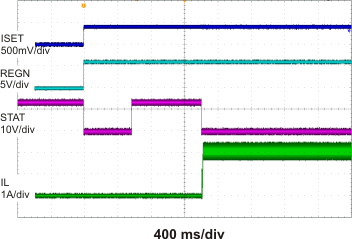
| Figure 2 | Charge Enable by ISET | |||
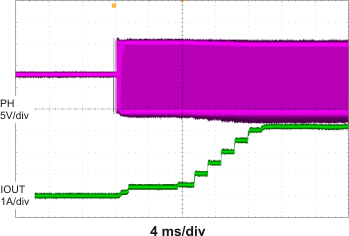
| Figure 3 | Current Soft Start | |||
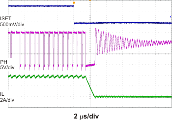
| Figure 4 | Charge Disable by ISET | |||
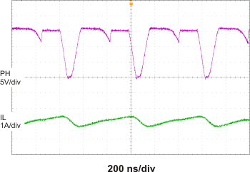
| Figure 5 | Continuous Conduction Mode Switching | |||
| Figure 6 | Discontinuous Conduction Mode Switching | |||
| Figure 7 | BATFET to ACFET Transition during Power Up | |||
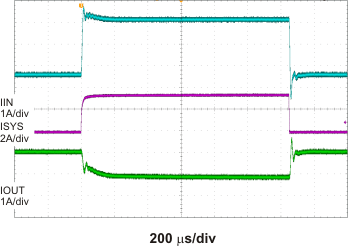
| Figure 8 | System Load Transient (Input Current DPM) | |||
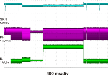
| Figure 9 | Battery Insertion and Removal | |||
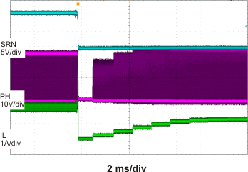
| Figure 10 | Battery to Ground Short Protection | |||
| Figure 11 | Battery to Ground Short Transition | |||
| Figure 12 | Efficiency vs Output Current (VIN = 15 V) | |||
| Figure 13 | Efficiency vs Output Current (VOUT = 3.8 V) | |||
(1) All waveforms and data are measured on HPA610 and HPA706 EVMs.

