SLUSAM9E July   2011  – April 2020 BQ76925

PRODUCTION DATA.  

  1. Features
  2. Applications
  3. Description
    1.     Device Images
      1.      Simplified Schematic
  4. Revision History
  5. Description (Continued)
  6. Pin Configuration and Functions
    1.     Pin Functions
  7. Specifications
    1. 7.1  Absolute Maximum Ratings
    2. 7.2  ESD Ratings
    3. 7.3  Recommended Operating Conditions
    4. 7.4  Thermal Information
    5. 7.5  Electrical Characteristics: Supply Current
    6. 7.6  Internal Power Control (Startup and Shutdown)
    7. 7.7  3.3-V Voltage Regulator
    8. 7.8  Voltage Reference
    9. 7.9  Cell Voltage Amplifier
    10. 7.10 Current Sense Amplifier
    11. 7.11 Overcurrent Comparator
    12. 7.12 Internal Temperature Measurement
    13. 7.13 Cell Balancing and Open Cell Detection
    14. 7.14 I2C Compatible Interface
    15. 7.15 Typical Characteristics
  8. Detailed Description
    1. 8.1 Overview
    2. 8.2 Functional Block Diagram
    3. 8.3 Feature Description
      1. 8.3.1 Internal LDO Voltage Regulator
      2. 8.3.2 ADC Interface
        1. 8.3.2.1 Reference Voltage
          1. 8.3.2.1.1 Host ADC Calibration
        2. 8.3.2.2 Cell Voltage Monitoring
          1. 8.3.2.2.1 Cell Amplifier Headroom Under Extreme Cell Imbalance
          2. 8.3.2.2.2 Cell Amplifier Headroom Under BAT Voltage Drop
        3. 8.3.2.3 Current Monitoring
        4. 8.3.2.4 Overcurrent Monitoring
        5. 8.3.2.5 Temperature Monitoring
          1. 8.3.2.5.1 Internal Temperature Monitoring
      3. 8.3.3 Cell Balancing and Open Cell Detection
    4. 8.4 Device Functional Modes
      1. 8.4.1 Power Modes
        1. 8.4.1.1 POWER ON RESET (POR)
        2. 8.4.1.2 STANDBY
        3. 8.4.1.3 SLEEP
    5. 8.5 Programming
      1. 8.5.1 Host Interface
        1. 8.5.1.1 I2C Addressing
        2. 8.5.1.2 Bus Write Command to BQ76925
        3. 8.5.1.3 Bus Read Command from BQ76925 Device
    6. 8.6 Register Maps
      1. 8.6.1 Register Descriptions
  9. Application and Implementation
    1. 9.1 Application Information
      1. 9.1.1 Recommended System Implementation
        1. 9.1.1.1 Voltage, Current, and Temperature Outputs
        2. 9.1.1.2 Power Management
        3. 9.1.1.3 Low Dropout (LDO) Regulator
        4. 9.1.1.4 Input Filters
        5. 9.1.1.5 Output Filters
      2. 9.1.2 Cell Balancing
    2. 9.2 Typical Application
      1. 9.2.1 Design Requirements
      2. 9.2.2 Detailed Design Procedure
      3. 9.2.3 Application Curves
  10. 10Power Supply Recommendations
  11. 11Layout
    1. 11.1 Layout Guidelines
    2. 11.2 Layout Example
  12. 12Device and Documentation Support
    1. 12.1 Documentation Support
      1. 12.1.1 Related Documentation
    2. 12.2 Receiving Notification of Documentation Updates
    3. 12.3 Support Resources
    4. 12.4 Trademarks
    5. 12.5 Electrostatic Discharge Caution
    6. 12.6 Glossary
  13. 13Mechanical, Packaging, and Orderable Information

Low Dropout (LDO) Regulator

When the LDO load current is higher than 4 mA, the LDO must be used with an external pass transistor. In this configuration, a high-gain bypass device is recommended. ZXTP25040DFH and IRLML9303 are example transistors. A Z1 diode is recommended to protect the gate-source or base emitter of the bypass transistor.

Adding the RV3P3 and CV3P3-2 filter helps to isolate the load from the V3P3 transient caused by the load and the transients on BAT.
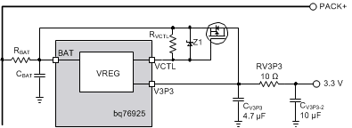
BQ76925 ldo_filters_lusam9.gifFigure 15. LDO Regulator