SLUSAO7C September   2011  – July 2024 UCC28063

PRODUCTION DATA  

  1.   1
  2. Features
  3. Applications
  4. Description
  5. Revision History
  6. Pin Configuration and Functions
  7. Specifications
    1. 6.1 Absolute Maximum Ratings
    2. 6.2 ESD Ratings
    3. 6.3 Recommended Operating Conditions
    4. 6.4 Thermal Information
    5. 6.5 Electrical Characteristics
    6. 6.6 Typical Characteristics
  8. Detailed Description
    1. 7.1 Overview
    2. 7.2 Functional Block Diagram
    3. 7.3 Feature Description
      1. 7.3.1  Principles of Operation
      2. 7.3.2  Natural Interleaving
      3. 7.3.3  On-Time Control, Maximum Frequency Limiting, and Restart Timer
      4. 7.3.4  Distortion Reduction
      5. 7.3.5  Zero-Current Detection and Valley Switching
      6. 7.3.6  Phase Management and Light-Load Operation
      7. 7.3.7  External Disable
      8. 7.3.8  Improved Error Amplifier
      9. 7.3.9  Soft Start
      10. 7.3.10 Brownout Protection
      11. 7.3.11 Dropout Detection
      12. 7.3.12 VREF
      13. 7.3.13 VCC
      14. 7.3.14 Control of Downstream Converter
      15. 7.3.15 System Level Protections
        1. 7.3.15.1 Failsafe OVP - Output Overvoltage Protection
        2. 7.3.15.2 Overcurrent Protection
        3. 7.3.15.3 Open-Loop Protection
        4. 7.3.15.4 VCC Undervoltage Lock-Out (UVLO) Protection
        5. 7.3.15.5 Phase-Fail Protection
        6. 7.3.15.6 CS-Open, TSET-Open and -Short Protection
        7. 7.3.15.7 Thermal Shutdown Protection
        8. 7.3.15.8 AC-Line Brownout and Dropout Protections
        9. 7.3.15.9 Fault Logic Diagram
    4. 7.4 Device Functional Modes
  9. Applications and Implementation
    1. 8.1 Application Information
    2. 8.2 Typical Application
      1. 8.2.1 Design Requirements
      2. 8.2.2 Detailed Design Procedure
        1. 8.2.2.1  Inductor Selection
        2. 8.2.2.2  ZCD Resistor Selection (RZA, RZB)
        3. 8.2.2.3  HVSEN
        4. 8.2.2.4  Output Capacitor Selection
        5. 8.2.2.5  Selecting (RS) For Peak Current Limiting
        6. 8.2.2.6  Power Semiconductor Selection (Q1, Q2, D1, D2)
        7. 8.2.2.7  Brownout Protection
        8. 8.2.2.8  Converter Timing
        9. 8.2.2.9  Programming VOUT
        10. 8.2.2.10 Voltage Loop Compensation
      3. 8.2.3 Application Curves
        1. 8.2.3.1 Input Ripple Current Cancellation with Natural Interleaving
        2. 8.2.3.2 Brownout Protection
  10. Power Supply Recommendations
  11. 10Layout
    1. 10.1 Layout Guidelines
    2. 10.2 Layout Example
  12. 11Device and Documentation Support
    1. 11.1 Device Support
      1. 11.1.1 Development Support
        1. 11.1.1.1 Related Parts
      2. 11.1.2 Device Nomenclature
        1. 11.1.2.1 Detailed Pin Description
    2. 11.2 Documentation Support
      1. 11.2.1 Related Documentation
    3. 11.3 Trademarks
    4. 11.4 Electrostatic Discharge Caution
    5. 11.5 Glossary
  13. 12Mechanical, Packaging, and Orderable Information

Typical Characteristics

At VCC = 16 V, AGND = PGND = 0 V, VINAC = 3 V, VSENSE = 6 V, HVSEN = 3 V, PHB = 5 V, RTSET = 133 kΩ; all voltages are with respect to GND, all outputs unloaded, TJ = TA = +25 °C, and currents are positive into and negative out of the specified terminal, unless otherwise noted.
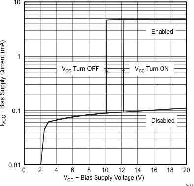
UCC28063 Bias
                        Supply Current vs Bias Supply Voltage
Figure 6-1 Bias Supply Current vs Bias Supply Voltage
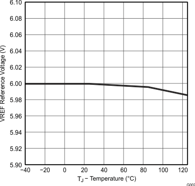
UCC28063 Reference Voltage vs Temperature
IVREF = 0 to –2 mA
Figure 6-3 Reference Voltage vs Temperature
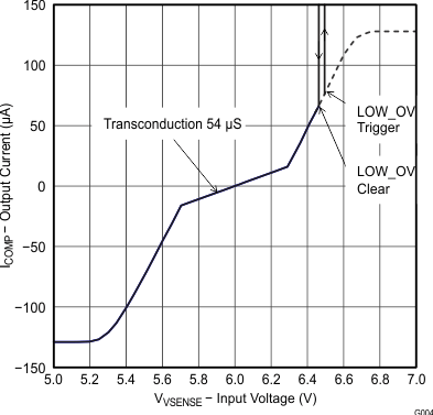
UCC28063 Error
                        Amplifier Output Current vs Input Voltage
Soft-Start Completed
Figure 6-5 Error Amplifier Output Current vs Input Voltage
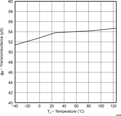
UCC28063 Error
                        Amplifier Transconductance vs Temperature
5.9 V < VVSENSE < 6.1 V
Figure 6-7 Error Amplifier Transconductance vs Temperature
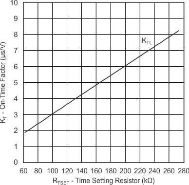
UCC28063 On-Time Factor vs Time Setting Resistor
Figure 6-9 On-Time Factor vs Time Setting Resistor
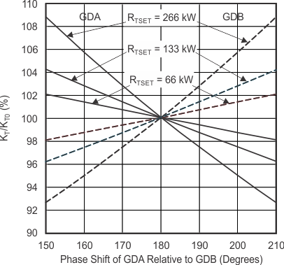
UCC28063 On-Time Factor vs Phase Error
KTO = 2(KTA × KTB) / KTA + KTB
Figure 6-11 On-Time Factor vs Phase Error
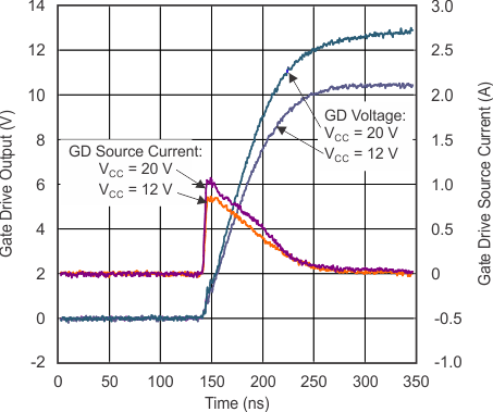
UCC28063 Gate
                        Drive Rising vs Time
CLOAD = 4.7 nF
Figure 6-13 Gate Drive Rising vs Time
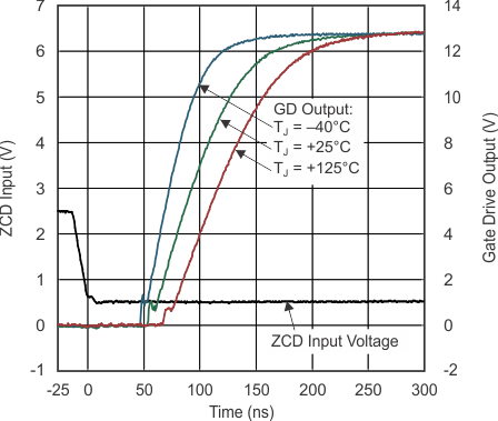
UCC28063 Gate
                        Drive Rising and Delay From ZCD Input vs Time
CLOAD = 4.7 nF
Figure 6-15 Gate Drive Rising and Delay From ZCD Input vs Time
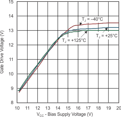
UCC28063 Gate
                        Drive Output High vs VCC
RLOAD = 2.7 kΩ
Figure 6-17 Gate Drive Output High vs VCC
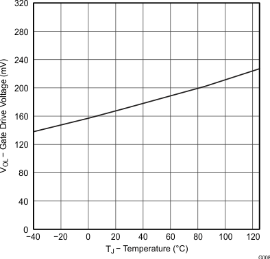
UCC28063 Gate
                        Drive Low Voltage vs Temperature
Load = 100 mA
Figure 6-19 Gate Drive Low Voltage vs Temperature
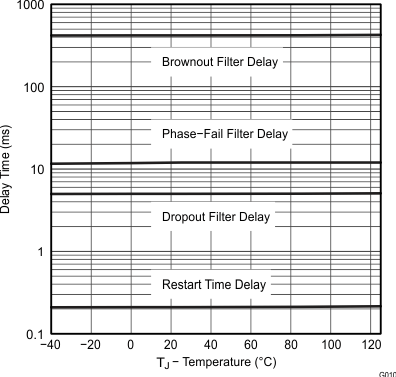
UCC28063 Various Delay Times vs Temperature
Figure 6-21 Various Delay Times vs Temperature
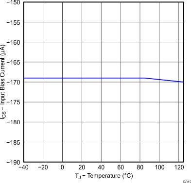
UCC28063 Current Sense Input Bias Current vs Temperature
VCS = –195 mV
Figure 6-23 Current Sense Input Bias Current vs Temperature
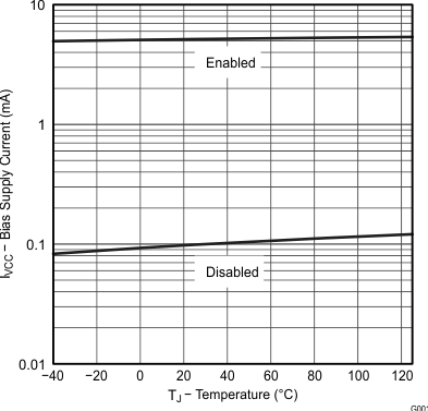
UCC28063 Bias
                        Supply Current vs Temperature
Figure 6-2 Bias Supply Current vs Temperature
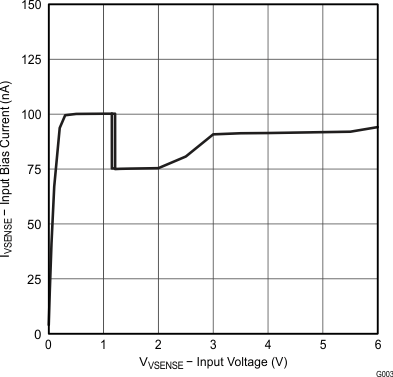
UCC28063 VSENSE Input Bias Current vs Input Voltage
Figure 6-4 VSENSE Input Bias Current vs Input Voltage
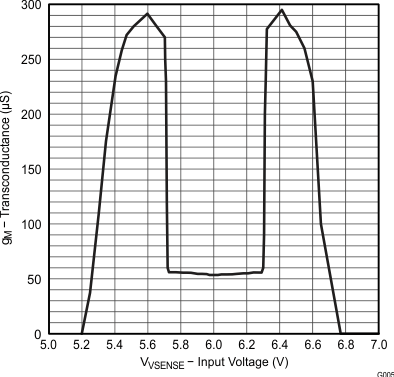
UCC28063 Error
                        Amplifier Transconductance vs VSENSE
Figure 6-6 Error Amplifier Transconductance vs VSENSE
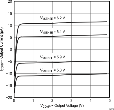
UCC28063 Error
                        Amplifier Output Current vs Output Voltage
Figure 6-8 Error Amplifier Output Current vs Output Voltage
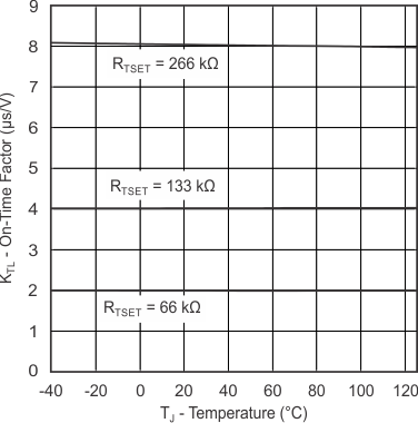
UCC28063 On-Time Factor Phase A and B vs Temperature
Figure 6-10 On-Time Factor Phase A and B vs Temperature
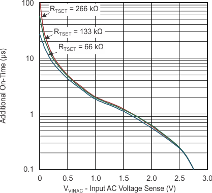
UCC28063 Additional On Time vs VINAC
Figure 6-12 Additional On Time vs VINAC
UCC28063 Gate
                        Drive Falling vs Time
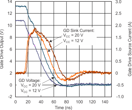
CLOAD = 4.7 nF
Figure 6-14 Gate Drive Falling vs Time
UCC28063 Gate
                        Drive Falling and Delay From CS Input vs Time
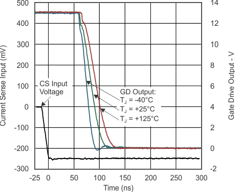
CLOAD = 4.7 nF
Figure 6-16 Gate Drive Falling and Delay From CS Input vs Time
UCC28063 Gate
                        Drive High Voltage vs Temperature
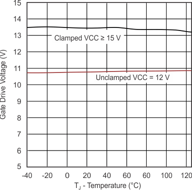
RLOAD = 2.7 kΩ
Figure 6-18 Gate Drive High Voltage vs Temperature
UCC28063 Gate
                        Drive Low Voltage in UVLO vs Bias Supply Voltage
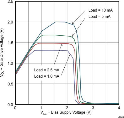
Figure 6-20 Gate Drive Low Voltage in UVLO vs Bias Supply Voltage
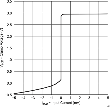
UCC28063 Zero
                        Current Detect Clamp Voltage vs Input Current
Figure 6-22 Zero Current Detect Clamp Voltage vs Input Current
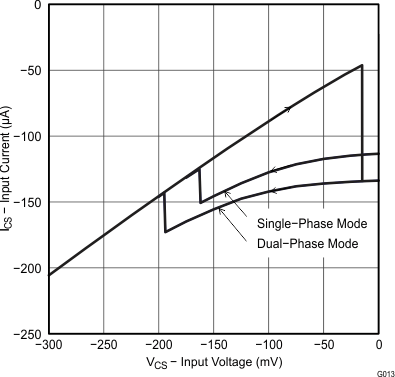
UCC28063 Current Sense Input Bias Current vs Input Voltage
Figure 6-24 Current Sense Input Bias Current vs Input Voltage