SLUSAO7C September 2011 – July 2024 UCC28063
PRODUCTION DATA
- 1
- 1 Features
- 2 Applications
- 3 Description
- 4 Revision History
- 5 Pin Configuration and Functions
- 6 Specifications
-
7 Detailed Description
- 7.1 Overview
- 7.2 Functional Block Diagram
- 7.3
Feature Description
- 7.3.1 Principles of Operation
- 7.3.2 Natural Interleaving
- 7.3.3 On-Time Control, Maximum Frequency Limiting, and Restart Timer
- 7.3.4 Distortion Reduction
- 7.3.5 Zero-Current Detection and Valley Switching
- 7.3.6 Phase Management and Light-Load Operation
- 7.3.7 External Disable
- 7.3.8 Improved Error Amplifier
- 7.3.9 Soft Start
- 7.3.10 Brownout Protection
- 7.3.11 Dropout Detection
- 7.3.12 VREF
- 7.3.13 VCC
- 7.3.14 Control of Downstream Converter
- 7.3.15
System Level Protections
- 7.3.15.1 Failsafe OVP - Output Overvoltage Protection
- 7.3.15.2 Overcurrent Protection
- 7.3.15.3 Open-Loop Protection
- 7.3.15.4 VCC Undervoltage Lock-Out (UVLO) Protection
- 7.3.15.5 Phase-Fail Protection
- 7.3.15.6 CS-Open, TSET-Open and -Short Protection
- 7.3.15.7 Thermal Shutdown Protection
- 7.3.15.8 AC-Line Brownout and Dropout Protections
- 7.3.15.9 Fault Logic Diagram
- 7.4 Device Functional Modes
-
8 Applications and Implementation
- 8.1 Application Information
- 8.2
Typical Application
- 8.2.1 Design Requirements
- 8.2.2
Detailed Design Procedure
- 8.2.2.1 Inductor Selection
- 8.2.2.2 ZCD Resistor Selection (RZA, RZB)
- 8.2.2.3 HVSEN
- 8.2.2.4 Output Capacitor Selection
- 8.2.2.5 Selecting (RS) For Peak Current Limiting
- 8.2.2.6 Power Semiconductor Selection (Q1, Q2, D1, D2)
- 8.2.2.7 Brownout Protection
- 8.2.2.8 Converter Timing
- 8.2.2.9 Programming VOUT
- 8.2.2.10 Voltage Loop Compensation
- 8.2.3 Application Curves
- 9 Power Supply Recommendations
- 10Layout
- 11Device and Documentation Support
- 12Mechanical, Packaging, and Orderable Information
3 Description
Optimized for consumer applications concerned with audible noise elimination, this solution extends the advantages of transition mode – high efficiency with low-cost components – to higher power ratings than previously possible. By utilizing a Natural Interleaving™ technique, both channels operate as masters (that is, there is no slave channel) synchronized to the same frequency. This approach delivers inherently strong matching, faster responses, and ensures that each channel operates in transition mode.
Expanded system level protections feature input brownout and dropout recovery, output over-voltage, open-loop, overload, soft-start, phase-fail detection, and thermal shutdown. The additional FailSafe over-voltage protection (OVP) feature protects against shorts to an intermediate voltage that, if undetected, could lead to catastrophic device failure. Advanced non-linear gain results in rapid, yet smoother response to line and load transient events. Reduced bias currents improve stand-by power efficiency. Special line-dropout handling avoids significant current disruption and minimizes audible-noise generation.
| PART NUMBER | PACKAGE | BODY SIZE (NOM) |
|---|---|---|
| UCC28063 | SOIC (16) | 9.90 mm × 3.91 mm |
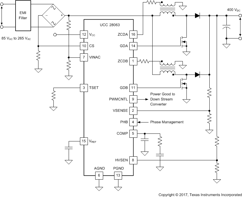
 Typical Application Diagram
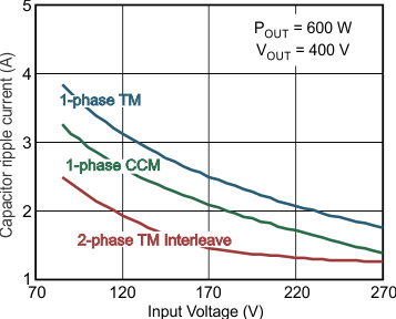
 Input Ripple Current Reduction with Interleaving